Reverse Engineering PCB
-
PCB Reverse Engineering and how to Reverse Engineer a PCB
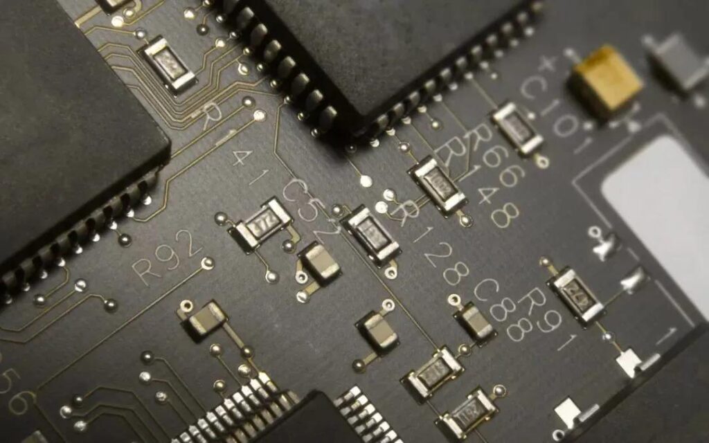
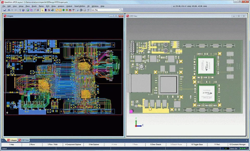
Reverse engineering plays an important role in industries in different sectors, mainly in the printed circuit boards. PCB Reverse Engineering is the multilayered process where there is inclusion of PCB research, reverse analysis and PCB design for r...
-
Clone PCB Board Component Layout Drawing
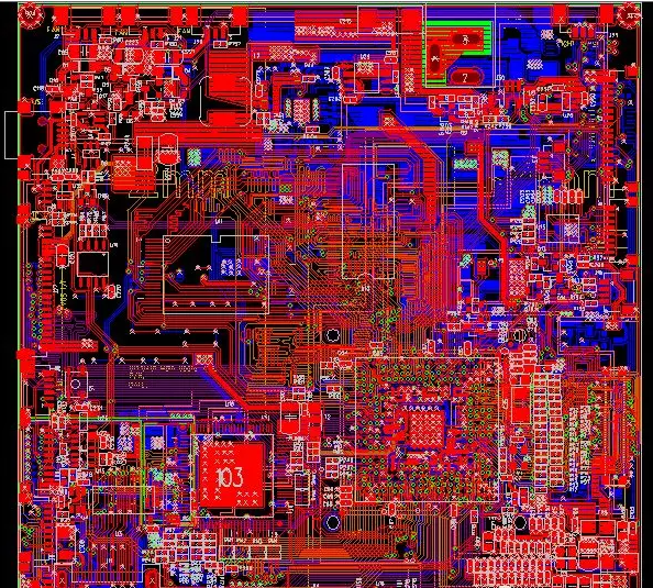
Clone PCB Board Component Layout Drawing is another very important step for PCB Clone service, below there are several points need to be clarified in the process: 1. Whether the layout of the components is dense and orderly, neatly arranged, and ...
-
Cloning PCB Board Process
During Cloning PCB Board process, after the printed circuit board schematic drawing recreation is completed, the PCB diagram should be reviewed to see whether the electronic PCB card relayout is reasonable and whether the optimal effect can be achie...
-
Clone Digital Circuit PCB Board Schematic
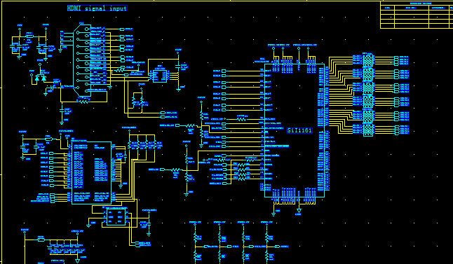
When we clone Digital Circuit PCB Board Schematic, the propagation of a digital signal is from one logic gate to another logic gate. The signal is sent from the output end to the receiving end through a wire. When we clone Digital Circuit PCB Bo...
-
GPS Module Circuit Board Reverse Engineering
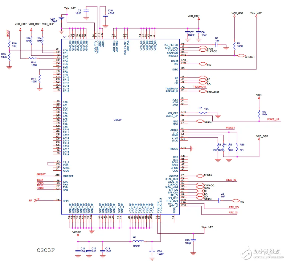
GPS Module Circuit Board Reverse Engineering can extract embedded schematic diagram out from it and then recreate layout drawing, netlist, Gerber file, list of components can be built according to the parts applied on it; GPS Module Circuit Board...
-
Projector Circuit Board Cloning
Projector Circuit Board Cloning is to help client re-manufacture the electronic PCB card of projector, hereby mainly refers to mainboard, restore PCB board layout diagram and gerber file in order to re-manufacture it; Projector Circuit Board Clon...
-
Projector PCB Board Reverse Engineering
Projector PCB Board Reverse Engineering will be able to extract schematic diagram, netlist from original printed circuit board, through schematic drawing to restore electronic projector circuit board layout diagram, gerber file, and de-solder the co...
-
Electronic PCB Board Gerber File Cloning
In high-speed Electronic PCB Board Gerber File Cloning, there will inevitably be parasitic inductance, parasitic resistance and parasitic capacitance, so the high-frequency noise will eventually be coupled to other circuits, and the presence of para...
-
Reverse Engineering PCB Board Layout Drawing Common Mistakes
There are some common mistakes in the process of Reverse Engineering PCB Board Layout Drawing, (1) There is no signal connected to the ERC report pin: I/O attributes are defined for the pins when the package is created, Inconsistent grid attr...
-
HDI Circuit Board Layout Cloning
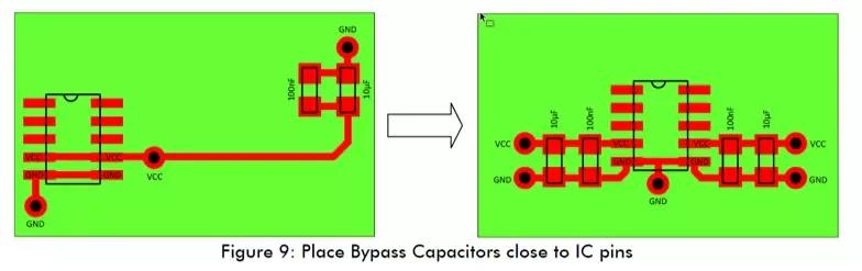
Digital circuits often require discontinuous currents, so inrush currents are generated for some HDI Circuit Board Layout cloning. If the power trace is very long, the presence of inrush current will cause high-frequency noise which can be effective...