

PCB Reverse Engineering and how to Reverse Engineer a PCB
Reverse engineering plays an important role in industries in different sectors, mainly in the printed circuit boards. PCB Reverse Engineering is the multilayered process where there is inclusion of PCB research, reverse analysis and PCB design for reproduction of technology.
Reverse Engineering in PCB is also important for identifying and obtaining products ‘design. The structural characteristics of products can also be identified using the process. In the production, the aim of PCB Reverse Engineering is to ensure there is the creation of products with similar characteristics but with different functionalities.
Why Reserve Engineer is significant?
Design principles in the production process are determined through PCB Reverse Engineering. It is important when an organization is not able to trace the design information of a given product. In most cases, the first process in PCB Reverse Engineering involves dissembling a sample PCB and then carrying out analysis to get the information needed.
After the analysis, a company can create a documentation on the product, which can be reviewed later by the other members of the organization. The information that can be obtained in such cases is used to manufacture others while at the same time keeping information for review in the future.
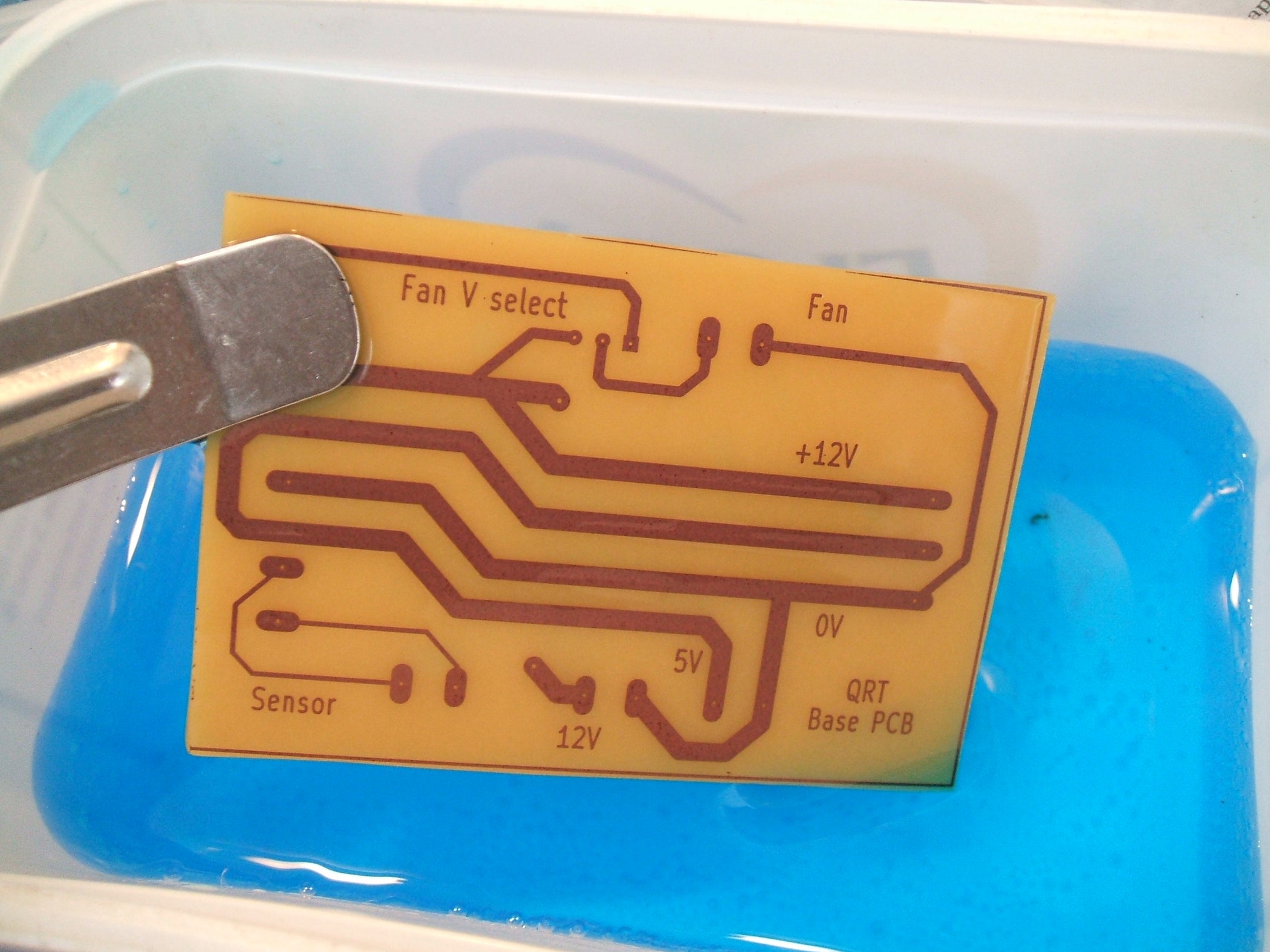
How to Reverse Engineer a PCB? Becoming a PCB reverse engineer isn’t so simple. There are three main steps one needs to take to achieve a functioning PCB without documentation or support. The first step is Reverse bound construction.
Photographs of both sides of the PC board are required to begin the process. The second step involves building the layout. This step takes plenty of hours and a lot of concentration. The last step is deriving a schematic. You need to combine both sides, label components with symbols, and arrange tracks so they make sense and are simple to interpret.
Tags: bakke ingeniørarbejde elektronisk pcb-kort gerber-fil,bakke ingeniørarbejde overordnet printkort layout design,bakke ingeniørarbejde trykt ledningskort skematisk fil