

What is PCB Reverse Engineering?
PCB (Printed Circuit Board) reverse engineering involves analyzing and understanding the design, layout, and functionality of a printed circuit board without access to its original design documents such ash gerber file or schematic diagrams. This process is often undertaken when the original documentation is unavailable, outdated, or incomplete.
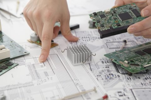
Reverse engineering a PCB typically involves several steps:
- Physical Examination: The first step involves physically examining the PCB, noting components, traces, connections, and any identifying marks or labels.
- Component Identification: Each component on the board is identified, noting its type, specifications, and connections. This may involve deciphering part numbers, datasheets, and identifying the role of each component within the circuit.
- Schematic Reconstruction: Reverse engineers attempt to reconstruct the schematic diagram of the PCB. This involves mapping out connections between components, identifying input and output points, and understanding the overall circuitry.
- Reverse-Designing the Layout: Understanding the physical placement of components, traces, and layers on the PCB is crucial. Sometimes, reverse engineers create a new PCB layout based on the information gathered.
- Functional Testing: Once the schematic and layout are reconstructed, functional testing is performed to ensure that the reverse-engineered design behaves as expected and matches the original functionality.
Reverse engineering a PCB can be a complex task that requires a combination of technical skills in electronics, PCB design, soldering, and sometimes specialized equipment like multimeters, oscilloscopes, and PCB layout software. It’s often employed in scenarios where replicating or modifying existing printed circuit board is necessary, or when troubleshooting and repairing legacy systems without documentation.