"Everything we build starts with design engineering. CECL manufactured boards for one of our products. It went perfectly – a real success.It is really an high quality service they have provided to us!"
By Nile Smith from Sinotech Inc.
“We had several very old device with obsolete boards need to be replaced –through CECL professional service.We got what we needed, and we’ve been using the results of the work without any problem till now.”
By Richard Anderson from TWP system Inc.
"Guys from CECL manufacture PCBs we use in one of our products, a clinometer and we’ve never had a problem with anything. The boards come in, they work. And, their team is very responsive."
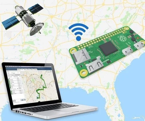
Die detaillierte Dokumentationsprüfung ist eine der intensivsten Phasen der Leiterplatten-Reverse-Engineering-Analyse. Ingenieure müssen Schaltplan, Netzliste, Layoutzeichnung und Stückliste mit höchster Präzision extrahieren und verifizieren. In dieser Phase werden hochdichte BGA-Mikrocontroller, GNSS-Empfänger, SIM-Schnittstellen, CAN- oder UART-Kommunikationsleitungen und Spannungsregelungsschaltungen sorgfältig nachverfolgt, um die korrekten logischen Beziehungen wiederherzustellen. Die ermittelte Netzliste wird mit den physischen Kupferverbindungen abgeglichen, um sicherzustellen, dass die duplizierte oder nachgebildete Konstruktion die Signalkontinuität und Impedanzkontrolle beibehält. Die Generierung einer präzisen Gerber-Datei aus den analysierten Lagen ist kein einfacher Kopiervorgang; sie beinhaltet die Validierung der Leiterbahnbreite, der HF-Erdungsisolierung, der Antennenanpassungsnetzwerke und der Parameter des mehrlagigen Aufbaus. Um Risiken zu minimieren und sicherzustellen, dass jeder ermittelte Schaltplan exakt dem gemessenen Spannungs- und Kommunikationsverhalten entspricht, führen die Prüfteams häufig separates Reverse Engineering jedes Funktionsblocks durch. Dieser systematische Ansatz unterstützt zuverlässige Reproduktions- und Wiederaufbereitungsprozesse für GPS-Tracking-Module, die in anspruchsvollen Baustellenumgebungen eingesetzt werden.
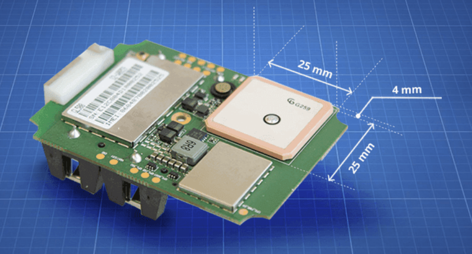
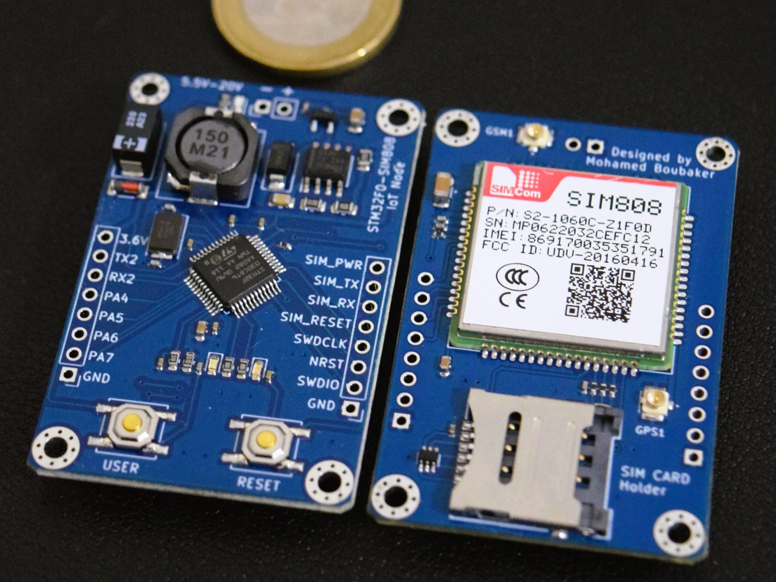
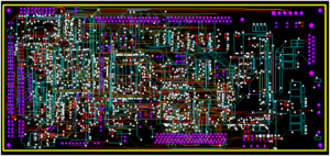
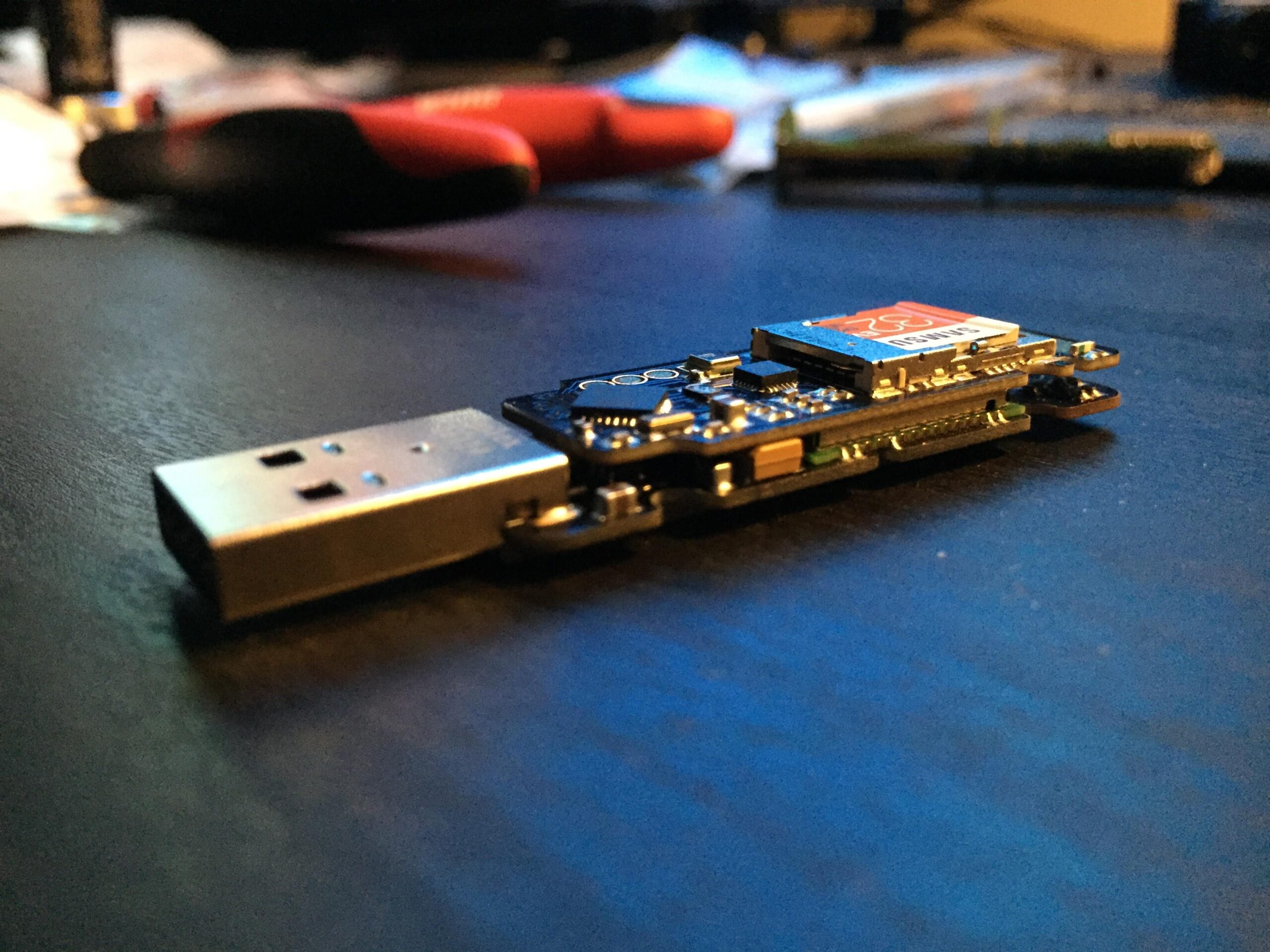
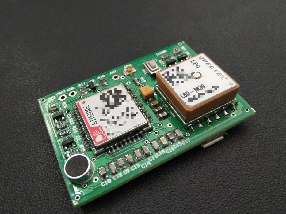
In-depth documentation inspection is one of the most intensive phases of PCB reverse engineering inspection. Engineers must extract and verify the schematic diagram, netlist, layout drawing, and bom list with high precision. During this stage, high-density BGA microcontrollers, GNSS receivers, SIM interfaces, CAN or UART communication lines, and power regulation circuits are carefully traced to recreate accurate logical relationships. The recovered netlist is cross-checked against physical copper connectivity to ensure that the duplicate or replicate design maintains signal continuity and impedance control. Generating a precise Gerber file from analyzed layers is not simply a copy process; it involves validating track width, RF grounding isolation, antenna matching networks, and multi-layer stack-up parameters. Inspection teams often reverse engineering each functional block separately to reduce risk, ensuring that every recovered schematic diagram corresponds exactly to measured voltage and communication behavior. This disciplined approach supports reliable reproduce and remanufacture processes for GPS tracking modules used in demanding construction environments.
गहराई से डॉक्यूमेंटेशन इंस्पेक्शन, PCB रिवर्स इंजीनियरिंग इंस्पेक्शन के सबसे इंटेंसिव फेज़ में से एक है। इंजीनियरों को स्कीमैटिक डायग्राम, नेटलिस्ट, लेआउट ड्रॉइंग और बॉम लिस्ट को हाई प्रिसिजन के साथ निकालना और वेरिफाई करना होता है। इस स्टेज के दौरान, हाई-डेंसिटी BGA माइक्रोकंट्रोलर, GNSS रिसीवर, SIM इंटरफेस, CAN या UART कम्युनिकेशन लाइन और पावर रेगुलेशन सर्किट को ध्यान से ट्रेस किया जाता है ताकि सटीक लॉजिकल रिलेशनशिप फिर से बनाए जा सकें। रिकवर की गई नेटलिस्ट को फिजिकल कॉपर कनेक्टिविटी से क्रॉस-चेक किया जाता है ताकि यह पक्का हो सके कि डुप्लिकेट या रेप्लिकेट डिज़ाइन सिग्नल कंटिन्यूटी और इम्पीडेंस कंट्रोल बनाए रखे। एनालाइज़ की गई लेयर से एक सटीक Gerber फ़ाइल बनाना सिर्फ़ एक कॉपी प्रोसेस नहीं है; इसमें ट्रैक की चौड़ाई, RF ग्राउंडिंग आइसोलेशन, एंटीना मैचिंग नेटवर्क और मल्टी-लेयर स्टैक-अप पैरामीटर को वैलिडेट करना शामिल है। इंस्पेक्शन टीमें अक्सर रिस्क कम करने के लिए हर फंक्शनल ब्लॉक की अलग से रिवर्स इंजीनियरिंग करती हैं, यह पक्का करते हुए कि हर रिकवर किया गया स्कीमैटिक डायग्राम मापे गए वोल्टेज और कम्युनिकेशन बिहेवियर से बिल्कुल मेल खाता हो। यह डिसिप्लिन्ड अप्रोच डिमांडिंग कंस्ट्रक्शन एनवायरनमेंट में इस्तेमाल होने वाले GPS ट्रैकिंग मॉड्यूल के लिए भरोसेमंद रिप्रोड्यूस और रीमैन्युफैक्चर प्रोसेस को सपोर्ट करता है।
Component verification and functional inspection represent another dense keyword-focused stage of the process. The bom list must be thoroughly validated, especially for RF chips, memory devices, and cellular communication modules that may have firmware dependencies. Engineers recover part numbers, confirm package footprints, and assess lifecycle availability before proceeding to clone or copy production. If certain components are obsolete, redesign or redevelopment planning begins at the inspection phase, ensuring compatibility while preserving original functionality. During reverse engineering inspection, teams often restore damaged traces, recreate missing reference designators, and refurbish corroded pads to obtain complete structural data. Electrical probing, signal capture, and communication testing confirm whether the recovered netlist and schematic diagram truly reflect real-time module operation. Only after comprehensive verification can the duplicate or reproduce stage move forward with confidence, minimizing technical deviation during remanufacture.
L’ispezione approfondita della documentazione è una delle fasi più intensive dell’ispezione di reverse engineering dei PCB. Gli ingegneri devono estrarre e verificare lo schema elettrico, la netlist, il disegno del layout e la distinta base con elevata precisione. Durante questa fase, microcontrollori BGA ad alta densità, ricevitori GNSS, interfacce SIM, linee di comunicazione CAN o UART e circuiti di regolazione della potenza vengono attentamente tracciati per ricreare relazioni logiche accurate. La netlist recuperata viene confrontata con la connettività fisica in rame per garantire che il progetto duplicato o replicato mantenga la continuità del segnale e il controllo dell’impedenza. Generare un file Gerber preciso dai livelli analizzati non è semplicemente un processo di copia; implica la convalida della larghezza di traccia, dell’isolamento di messa a terra RF, delle reti di adattamento dell’antenna e dei parametri di stack-up multistrato. I team di ispezione spesso eseguono il reverse engineering di ogni blocco funzionale separatamente per ridurre i rischi, garantendo che ogni schema elettrico recuperato corrisponda esattamente alla tensione misurata e al comportamento di comunicazione. Questo approccio disciplinato supporta processi di riproduzione e rifabbricazione affidabili per i moduli di tracciamento GPS utilizzati in ambienti di costruzione impegnativi.
The final stage of PCB board reverse engineering inspection focuses on reliability validation and production readiness. Once engineers recreate the layout drawing and generate the finalized Gerber file, the inspection team evaluates manufacturing tolerances, impedance requirements, and RF shielding effectiveness. For GPS tracking and telematics modules in wheel loaders, vibration resistance, temperature stability, and electromagnetic compatibility are critical performance factors. Inspection protocols therefore include simulated load testing, communication stability analysis, and power fluctuation monitoring. Any discovered inconsistencies between the restored design and actual system behavior trigger controlled redesign to optimize robustness without altering core architecture. By integrating recover, restore, replicate, and reproduce methodologies within a strict inspection framework, companies can confidently remanufacture high-performance telematics PCBs. A comprehensive PCB board reverse engineering inspection not only ensures technical accuracy but also strengthens SEO visibility when supported by detailed documentation keywords such as schematic diagram, netlist, bom list, layout drawing, and Gerber file. This systematic strategy ultimately supports sustainable maintenance, cost reduction, and long-term operational reliability for modern wheel loader fleets.
PCB Board Reverse Engineering Inspection means the circuit board documents extracted from physical sample must be checked to ensure the accuracy of the PCB file cloning.
PCB Board Reverse Engineering Inspection means the circuit board documents extracted from physical sample must be checked to ensure the accuracy of the PCB file cloning.
PCB Board reverse engineering need to check the circuit pattern quality, electrical connection and track route stability and rationality. The items need to be checking include:
L’inspection documentaire approfondie est l’une des phases les plus exigeantes du contrôle par rétro-ingénierie des circuits imprimés. Les ingénieurs doivent extraire et vérifier avec une grande précision le schéma, la netlist, le plan d’implantation et la nomenclature. À cette étape, les microcontrôleurs BGA haute densité, les récepteurs GNSS, les interfaces SIM, les lignes de communication CAN ou UART et les circuits de régulation de puissance sont minutieusement analysés afin de recréer des relations logiques exactes. La netlist récupérée est comparée à la connectivité physique du cuivre pour garantir que la duplication ou la réplication préserve la continuité du signal et le contrôle d’impédance. La génération d’un fichier Gerber précis à partir des couches analysées ne se limite pas à une simple copie ; elle implique la validation de la largeur des pistes, de l’isolation de la masse RF, des réseaux d’adaptation d’antenne et des paramètres d’empilement multicouches. Les équipes d’inspection procèdent souvent à la rétro-ingénierie de chaque bloc fonctionnel séparément afin de réduire les risques et de garantir que chaque schéma récupéré corresponde exactement aux tensions et aux comportements de communication mesurés. Cette approche rigoureuse permet des processus de reproduction et de remanufacturation fiables pour les modules de suivi GPS utilisés dans des environnements de construction exigeants.
1 tracks can be short and straight without the sacrifice of functions when reverse engineering pcb board;
2 if the reverse engineering has followed the limitation rules for track width;
3 among the tracks, tracks and fixed holes, tracks and soldering pads, if sufficient space has been saved for them;
4 if all the tracks have already avoided the parallel tracks (include the component leads);
5 if the sharp angle has been avoid;
6 check if the schematic diagram is rational and correct;
7 check if all the component packages are all correct and rational;
8 strong and weak electricity distance and the space between blocked areas;
9 check the schematic and PCB drawing correspondingly to avoid the lost of netlist provided by pcb board reverse engineering;
10 if the footprint of component can match with physical sample;
11 if the placement of components when reverse engineering pcb board are all properly;
PCB tersine mühendislik incelemesinin en yoğun aşamalarından biri, detaylı dokümantasyon incelemesidir. Mühendisler, şematik diyagramı, netlisti, yerleşim çizimini ve malzeme listesini yüksek hassasiyetle çıkarmalı ve doğrulamalıdır. Bu aşamada, yüksek yoğunluklu BGA mikrodenetleyiciler, GNSS alıcıları, SIM arayüzleri, CAN veya UART iletişim hatları ve güç düzenleme devreleri, doğru mantıksal ilişkileri yeniden oluşturmak için dikkatlice izlenir. Kurtarılan netlist, kopyalanan veya tekrarlanan tasarımın sinyal sürekliliğini ve empedans kontrolünü koruduğundan emin olmak için fiziksel bakır bağlantısıyla çapraz kontrol edilir. Analiz edilen katmanlardan hassas bir Gerber dosyası oluşturmak sadece bir kopyalama işlemi değildir; iz genişliğinin, RF topraklama izolasyonunun, anten eşleştirme ağlarının ve çok katmanlı yığın parametrelerinin doğrulanmasını içerir. İnceleme ekipleri, riski azaltmak için genellikle her fonksiyonel bloğu ayrı ayrı tersine mühendislik yaparak, kurtarılan her şematik diyagramın ölçülen voltaj ve iletişim davranışına tam olarak karşılık geldiğinden emin olurlar. Bu disiplinli yaklaşım, zorlu inşaat ortamlarında kullanılan GPS takip modülleri için güvenilir yeniden üretim ve yeniden imalat süreçlerini destekler.