"Everything we build starts with design engineering. CECL manufactured boards for one of our products. It went perfectly – a real success.It is really an high quality service they have provided to us!"
By Nile Smith from Sinotech Inc.
“We had several very old device with obsolete boards need to be replaced –through CECL professional service.We got what we needed, and we’ve been using the results of the work without any problem till now.”
By Richard Anderson from TWP system Inc.
"Guys from CECL manufacture PCBs we use in one of our products, a clinometer and we’ve never had a problem with anything. The boards come in, they work. And, their team is very responsive."
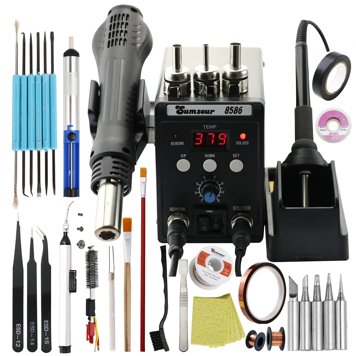
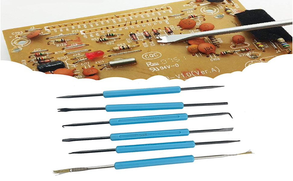
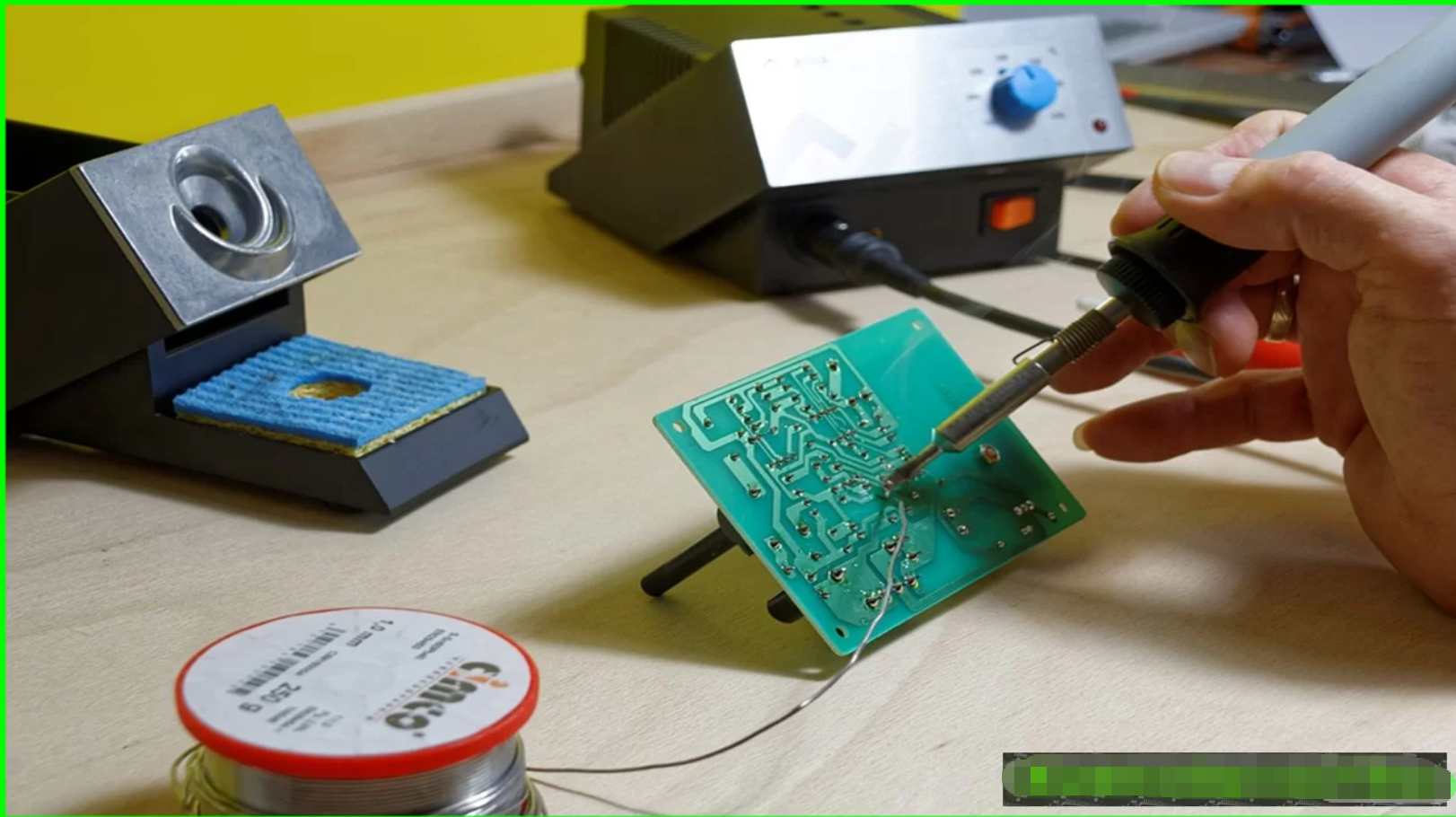
PCB reverse engineering relies on a systematic workflow supported by a combination of hardware inspection tools and software analysis platforms. At the earliest stage, visual and physical inspection tools are fundamental. High-resolution optical microscopes and digital inspection cameras are used to examine component markings, trace routing, via structures, and solder mask openings. For multilayer boards, X-ray inspection systems are critical tools, allowing engineers to identify internal layer stack-ups, buried vias, and hidden interconnections without destroying the board. In cases where deeper analysis is required, controlled depaneling, layer grinding, and polishing equipment are used to expose internal copper layers for accurate documentation. Precision measurement tools such as calipers and thickness gauges also support reverse engineering by helping determine board dimensions, dielectric thickness, and mechanical tolerances.
Das Reverse Engineering von Leiterplatten basiert auf einem systematischen Workflow, der durch eine Kombination aus Hardware-Inspektionswerkzeugen und Software-Analyseplattformen unterstützt wird. Visuelle und physikalische Inspektionswerkzeuge sind in der ersten Phase unerlässlich. Hochauflösende optische Mikroskope und digitale Inspektionskameras werden eingesetzt, um Bauteilmarkierungen, Leiterbahnführungen, Via-Strukturen und Lötstoppmaskenöffnungen zu untersuchen. Bei Multilayer-Leiterplatten sind Röntgeninspektionssysteme unverzichtbar, da sie es Ingenieuren ermöglichen, interne Lagenaufbauten, vergrabene Vias und verdeckte Verbindungen zu identifizieren, ohne die Leiterplatte zu zerstören. Für detailliertere Analysen werden Geräte zum kontrollierten Depaneling, zum Schleifen und Polieren der Lagen verwendet, um interne Kupferlagen für eine präzise Dokumentation freizulegen. PCB-CAD-Software wie Altium Designer, Cadence Allegro oder PADS dient dazu, Schaltplan, Layoutzeichnung und Gerber-Datei anhand der erfassten Daten zu rekonstruieren. Spezielle Reverse-Engineering-Software und Bildverarbeitungswerkzeuge helfen bei der Umwandlung gescannter Lagenbilder in bearbeitbare Vektordaten und verbessern so Genauigkeit und Effizienz erheblich. BOM-Management-Tools unterstützen die Bauteilidentifizierung, die Lebenszyklusanalyse und die Ersatzplanung, was für die Wiederaufbereitung oder das Redesign unerlässlich ist. Zusammen wandeln diese digitalen Werkzeuge Rohdaten aus der Inspektion in produktionsfertige Dokumentationen um und ermöglichen so ein zuverlässiges Reverse Engineering, Klonen, Aufarbeiten und Neuentwickeln von Leiterplatten für moderne Fertigungsanforderungen.
In recent days, pcb board reverse engineering tools have made some new breakthrough, some of the analysis tools have been developped regarding to the high speed design issue and pcb board reverse engineering. Take the software from INNOVEDA as the signal integrity analysis tool as reference, HYPERLYNX from this company has been charactered as easy to use, and can provide a powerful signal integrity analysis functions when reverse engineering pcb board. It has a very outstanding features is the user friendly operational interface which make the engineers can make analysis according to the their assumed scinerios when reverse engineering pcb board, and make the experiment on the terminal topology issues, through which the best solutions can be found after the features and reliability can be satisfied swiftly.
Il reverse engineering dei PCB si basa su un flusso di lavoro sistematico supportato da una combinazione di strumenti di ispezione hardware e piattaforme di analisi software. Nella fase iniziale, gli strumenti di ispezione visiva e fisica sono fondamentali. Microscopi ottici ad alta risoluzione e telecamere di ispezione digitali vengono utilizzati per esaminare le marcature dei componenti, il routing delle piste, le strutture dei fori di via e le aperture delle maschere di saldatura. Per le schede multistrato, i sistemi di ispezione a raggi X sono strumenti fondamentali, consentendo agli ingegneri di identificare sovrapposizioni di strati interni, fori di via interrati e interconnessioni nascoste senza distruggere la scheda. Nei casi in cui è richiesta un’analisi più approfondita, vengono utilizzate apparecchiature di depaneling controllato, levigatura e lucidatura degli strati per esporre gli strati di rame interni e ottenere una documentazione accurata. Software CAD per PCB come Altium Designer, Cadence Allegro o PADS vengono utilizzati per ricreare lo schema elettrico, il disegno del layout e il file Gerber in base ai dati raccolti. Software dedicati al reverse engineering dei PCB e strumenti di elaborazione delle immagini aiutano a convertire le immagini dei livelli scansionate in dati vettoriali modificabili, migliorando significativamente la precisione e l’efficienza. Gli strumenti di gestione della distinta base supportano l’identificazione dei componenti, l’analisi del ciclo di vita e la pianificazione delle sostituzioni, essenziali per la rigenerazione o la riprogettazione. Insieme, questi strumenti digitali trasformano i dati grezzi di ispezione in documentazione pronta per la produzione, consentendo un reverse engineering, una clonazione, un rinnovamento e una riqualificazione affidabili dei PCB per soddisfare i moderni requisiti di produzione.
As for those engineers who need to reverse engineering pcb board with high complexity and system, XTK signal integrity verification tools set from the INNOVEDA and signal integrity planning environment EPLANNER can provide a advanced algorithm and other more mature validation functions which can be used on the super speed signal integrity analysis of pcb board reverse engineering, include the topology analysis, high speed scanning or consumption, and other high level algorithm for signal integrity analysis.
In the past, engineers must make a choise between the HYPERLYNE and XTK when reverse engineering pcb board. In recent days, INNOVEDA can make the connections of these two tools of critical signal integrity scanning into realization, this connections can make the integrate together, and they can be used simutaneously when reverse engineering pcb board and consequently shorten the pcb board reverse engineering cycle. Generally speaking, HYPERLYNX has been used as the signal analysis tools for high speed PCB board reverse engineering, however, XTK and eplanner will be used to proceed the topology analysis and restricted terms when reverse engineering pcb board.
the supreme court has already proclaimed the business secret or intellectual property obtained from self-research or through reverse engineering PCB don’t belong to the unfair competition action. Circuit Engineering Co.,Ltd has commited to Reverse Engineering technology research and service for over two decades. and have ever reverse engineering then clone or copy the electronic printed circuit board from different industries, as well as the pcb board manufacture and prototype building. and we have great advantage over the PCB reverse engineering cycle control, research and development as well as the cost analysis.
La rétro-ingénierie des circuits imprimés repose sur un flux de travail systématique, s’appuyant sur une combinaison d’outils d’inspection matériels et de plateformes d’analyse logicielle. Dès les premières étapes, les outils d’inspection visuelle et physique sont essentiels. Des microscopes optiques haute résolution et des caméras d’inspection numériques permettent d’examiner le marquage des composants, le routage des pistes, les vias et les ouvertures du masque de soudure. Pour les cartes multicouches, les systèmes d’inspection par rayons X sont indispensables, permettant aux ingénieurs d’identifier l’empilement des couches internes, les vias enterrés et les interconnexions cachées sans endommager la carte. Lorsque des analyses plus approfondies sont nécessaires, des équipements de dépanelage contrôlé, de meulage et de polissage des couches sont utilisés pour exposer les couches de cuivre internes et obtenir une documentation précise. Les logiciels de CAO pour circuits imprimés, tels qu’Altium Designer, Cadence Allegro ou PADS, permettent de recréer le schéma, le plan d’implantation et le fichier Gerber à partir des données collectées. Des logiciels dédiés à la rétro-ingénierie des circuits imprimés et des outils de traitement d’images facilitent la conversion des images de couches numérisées en données vectorielles modifiables, améliorant considérablement la précision et l’efficacité. Les outils de gestion de la nomenclature (BOM) prennent en charge l’identification des composants, l’analyse du cycle de vie et la planification des substitutions, éléments essentiels pour la remanufacturation ou la reconception. Ensemble, ces outils numériques transforment les données d’inspection brutes en documentation prête pour la production, permettant une ingénierie inverse, un clonage, une remise à neuf et un redéveloppement fiables des circuits imprimés pour répondre aux exigences de la fabrication moderne.
Nowadays, electronic products are being updated in fast speed; and PCB reverse engineering from our company in the base of completely master the traditional PCB structure or its basic circuit, furthermore, is base upon the self research and development, include the software upgrade and product second phase development; and we will dedicate to clone PCB with 100% exact the same functions as original sample given by customers.at the same time, we also decrease the PCB reverse engineering cycle refers to the pcb board with blind or buried vias, effectively save customer time and energy, low down its cost. and which is also one of the reasons for us to be favor by most of our clients.
PCB tersine mühendisliği, donanım inceleme araçları ve yazılım analiz platformlarının bir kombinasyonuyla desteklenen sistematik bir iş akışına dayanır. En erken aşamada, görsel ve fiziksel inceleme araçları temel öneme sahiptir. Bileşen işaretlerini, iz yönlendirmesini, via yapılarını ve lehim maskesi açıklıklarını incelemek için yüksek çözünürlüklü optik mikroskoplar ve dijital inceleme kameraları kullanılır. Çok katmanlı kartlar için, X-ışını inceleme sistemleri kritik araçlardır ve mühendislerin kartı tahrip etmeden iç katman yığınlarını, gömülü via’ları ve gizli ara bağlantıları belirlemelerine olanak tanır. Daha derin analiz gerektiğinde, doğru dokümantasyon için iç bakır katmanlarını ortaya çıkarmak amacıyla kontrollü panel ayırma, katman taşlama ve parlatma ekipmanları kullanılır. Altium Designer, Cadence Allegro veya PADS gibi PCB CAD yazılımları, toplanan verilere dayanarak şematik diyagramı, yerleşim çizimini ve Gerber dosyasını yeniden oluşturmak için kullanılır. Özel PCB tersine mühendislik yazılımları ve görüntü işleme araçları, taranan katman görüntülerini düzenlenebilir vektör verilerine dönüştürmeye yardımcı olarak doğruluğu ve verimliliği önemli ölçüde artırır. BOM yönetim araçları, yeniden üretim veya yeniden tasarım için gerekli olan bileşen tanımlama, yaşam döngüsü analizi ve ikame planlamasını destekler. Bu dijital araçlar birlikte, ham denetim verilerini üretime hazır belgelere dönüştürerek, modern üretim gereksinimleri için güvenilir PCB tersine mühendisliği, klonlama, yenileme ve yeniden geliştirme olanağı sağlar.
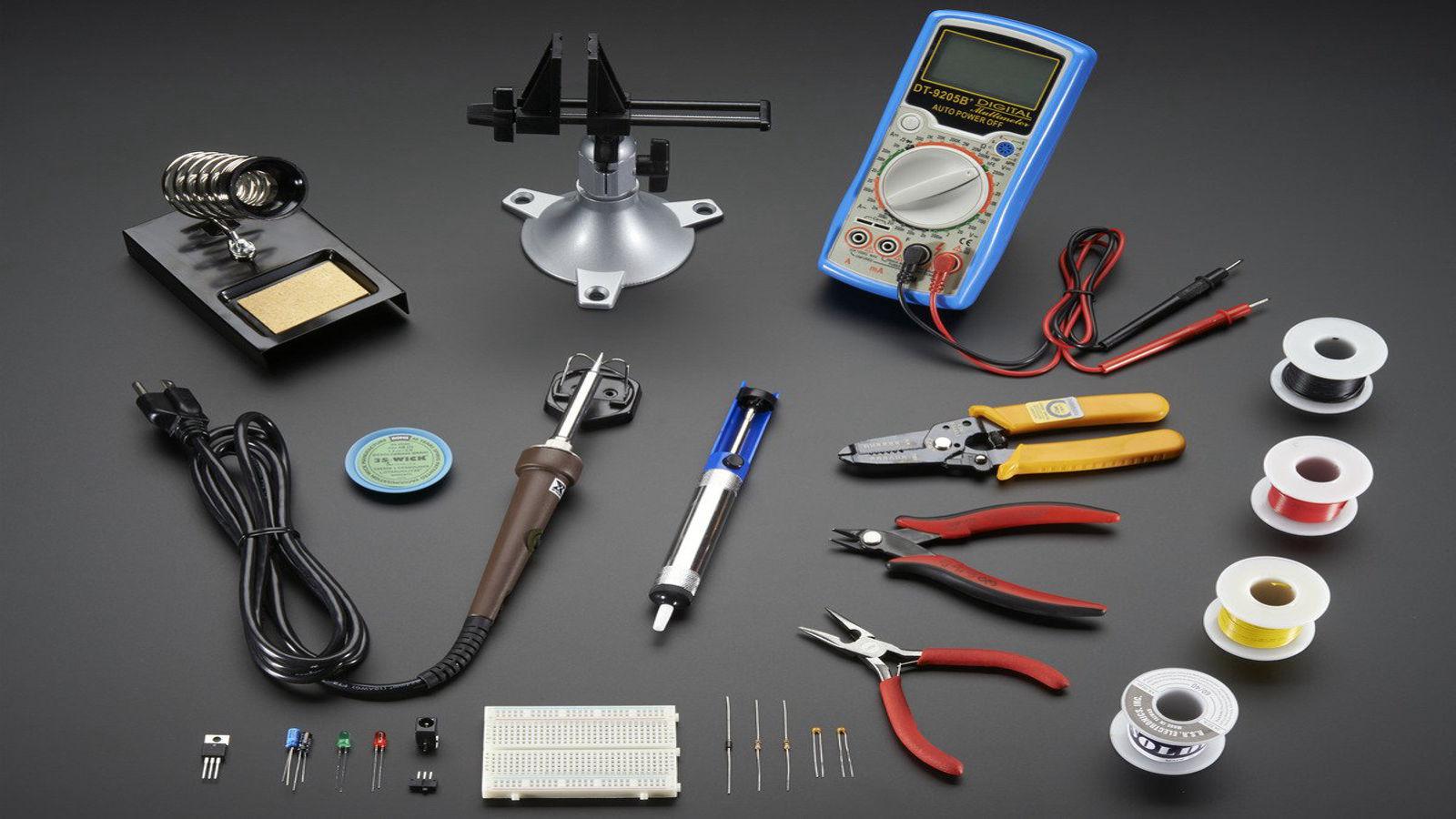
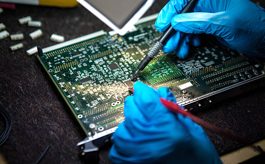
Once physical access is established, electrical and signal analysis tools become indispensable. Multimeters and LCR meters are used to identify passive component values, while curve tracers and semiconductor analyzers help characterize discrete devices. Oscilloscopes and logic analyzers are especially important when reverse engineering powered boards, as they allow engineers to observe clock signals, communication buses, and timing relationships. For high-speed or communication-focused PCBs, protocol analyzers for CAN, J1939, SPI, I²C, or UART provide insight into signal behavior and data flow. These tools help validate assumptions made during schematic reconstruction and ensure that the restored netlist accurately reflects real circuit functionality.
PCB रिवर्स इंजीनियरिंग एक सिस्टमैटिक वर्कफ़्लो पर निर्भर करती है, जिसे हार्डवेयर इंस्पेक्शन टूल्स और सॉफ्टवेयर एनालिसिस प्लेटफॉर्म के कॉम्बिनेशन से सपोर्ट मिलता है। शुरुआती स्टेज में, विज़ुअल और फिजिकल इंस्पेक्शन टूल्स बेसिक होते हैं। हाई-रिज़ॉल्यूशन ऑप्टिकल माइक्रोस्कोप और डिजिटल इंस्पेक्शन कैमरों का इस्तेमाल कंपोनेंट मार्किंग, ट्रेस रूटिंग, वाया स्ट्रक्चर और सोल्डर मास्क ओपनिंग की जांच करने के लिए किया जाता है। मल्टीलेयर बोर्ड के लिए, एक्स-रे इंस्पेक्शन सिस्टम बहुत ज़रूरी टूल्स हैं, जो इंजीनियरों को बोर्ड को खराब किए बिना इंटरनल लेयर स्टैक-अप, दबे हुए वाया और छिपे हुए इंटरकनेक्शन की पहचान करने में मदद करते हैं। जिन मामलों में ज़्यादा एनालिसिस की ज़रूरत होती है, उनमें सही डॉक्यूमेंटेशन के लिए इंटरनल कॉपर लेयर्स को दिखाने के लिए कंट्रोल्ड डीपैनलिंग, लेयर ग्राइंडिंग और पॉलिशिंग इक्विपमेंट का इस्तेमाल किया जाता है। इकट्ठा किए गए डेटा के आधार पर स्कीमैटिक डायग्राम, लेआउट ड्राइंग और गेरबर फ़ाइल को फिर से बनाने के लिए Altium Designer, Cadence Allegro, या PADS जैसे PCB CAD सॉफ्टवेयर का इस्तेमाल किया जाता है। खास PCB रिवर्स इंजीनियरिंग सॉफ्टवेयर और इमेज-प्रोसेसिंग टूल्स स्कैन की गई लेयर इमेज को एडिटेबल वेक्टर डेटा में बदलने में मदद करते हैं, जिससे एक्यूरेसी और एफिशिएंसी में काफी सुधार होता है। BOM मैनेजमेंट टूल्स कंपोनेंट आइडेंटिफिकेशन, लाइफसाइकल एनालिसिस और सब्स्टीट्यूशन प्लानिंग में मदद करते हैं, जो रीमैन्युफैक्चर या रीडिज़ाइन के लिए ज़रूरी है। साथ मिलकर, ये डिजिटल टूल्स रॉ इंस्पेक्शन डेटा को प्रोडक्शन-रेडी डॉक्यूमेंटेशन में बदल देते हैं, जिससे मॉडर्न मैन्युफैक्चरिंग ज़रूरतों के लिए भरोसेमंद PCB रिवर्स इंजीनियरिंग, क्लोनिंग, रिफर्बिशमेंट और रीडेवलपमेंट मुमकिन हो पाता है।
The final and most decisive category consists of software tools for documentation and data reconstruction. PCB CAD software such as Altium Designer, Cadence Allegro, or PADS is used to recreate the schematic diagram, layout drawing, and Gerber file based on collected data. Dedicated PCB reverse engineering software and image-processing tools assist in converting scanned layer images into editable vector data, significantly improving accuracy and efficiency. BOM management tools support component identification, lifecycle analysis, and substitution planning, which is essential for remanufacture or redesign. Together, these digital tools transform raw inspection data into production-ready documentation, enabling reliable PCB reverse engineering, cloning, refurbishment, and redevelopment for modern manufacturing requirements.