

Digital & Analog Ground Dividence in PCB Card Reverse Engineering
Digital & Analog Ground Dividence in PCB Card Reverse Engineering
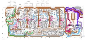
Digital & Analog Ground Dividence in PCB Card Reverse Engineering is critical since the existence of distributed inductance. Although they are connected in the PCB card layout, but the distance is long, it is different. On the same wire, the voltage at different points may be different, especially when the current is large. Because of the resistance of the wire, a voltage drop occurs when current flows. In addition, the wire also has a distributed inductance. Under the AC signal, the influence of the distributed inductance will be manifested.
Digital & Analog Ground Dividence in PCB Card Reverse Engineering
So we have to divide it into digital ground and analog ground, because the high frequency noise of the digital signal is very large. If the analog ground and the digital ground are mixed, the noise will be transmitted to the analog part, causing interference. If grounded separately, high frequency noise can be isolated by filtering at the power supply. But if the two grounds are mixed, it is not easy to filter.