


Printed Circuit Board Reverse Engineering Assemble Faulty
When a printed circuit board is reproduced from a cloned PCB design, assembly faults can sometimes occur even when the manufacturing process follows the supplied Gerber file. The phrase printed circuit board reverse engineering assemble faulty generally describes a situation in which a PCB manufactured from reverse-engineered Gerber data shows mis-conducts, abnormal operation, or improper performance after component assembly and soldering. Such problems do not necessarily mean that the PCB fabrication or assembly process itself is defective. In some cases, the underlying cause may be an inaccurate layout drawing, incorrect component footprint, missing connection, reversed polarity, or incomplete information recovered during PCB reverse engineering.
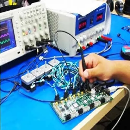
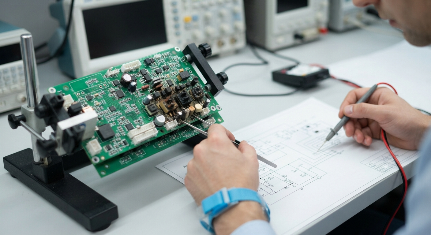
The first step in solving an assembly problem is to separate PCB manufacturing faults, soldering faults, and reverse engineering design errors. Engineers can begin by inspecting the assembled printed circuit board under magnification and comparing it against the original PCB card. Common assembly problems include insufficient solder, solder bridges, open joints, incorrect component orientation, misplaced components, and damaged pads. Electrical tests can then be performed to check continuity between critical nets and detect unexpected short circuits. If the physical assembly is correct but the electronic circuit board does not operate correctly, attention should move toward the reconstructed PCB design, including the schematic diagram, netlist, layout drawing, and Gerber file.
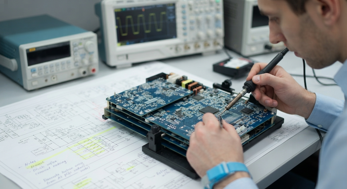
If the investigation indicates that the problem originates from the PCB reverse engineering process, the reconstructed design must be reviewed systematically. Engineers should compare the reverse-engineered layout drawing against the original board, checking copper tracks, vias, component positions, pad dimensions, layer-to-layer connections, and power or ground distribution. Particular attention should be given to multilayer PCB boards because internal traces cannot always be confirmed through visual inspection alone.
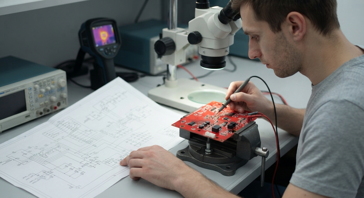
The Gerber data should also be regenerated from the corrected CAD file rather than manually modifying isolated manufacturing layers. At the same time, the BOM list and component footprints should be reviewed to ensure that the assembled components correspond exactly to the recovered design. This process can identify whether the original PCB was incorrectly interpreted during reverse engineering or whether the fault was introduced later during fabrication and assembly.
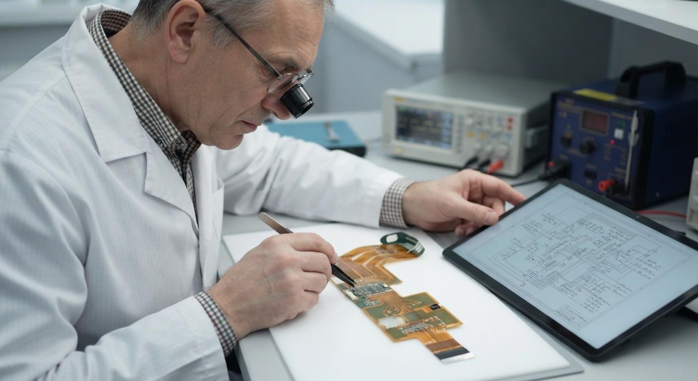
After identifying an error, engineers can modify the PCB layout and create a corrected prototype for verification. For example, an incorrectly routed signal can be transferred to the proper net, an incorrect footprint can be replaced, or a missing via can be added to restore connectivity. The revised CAD file is then used to generate a new Gerber file, followed by PCB fabrication and controlled assembly. Electrical testing should compare the corrected prototype with the original board under identical operating conditions. Where possible, functional testing, continuity testing, resistance measurements, and signal analysis can be used to confirm that the correction has solved the original problem.
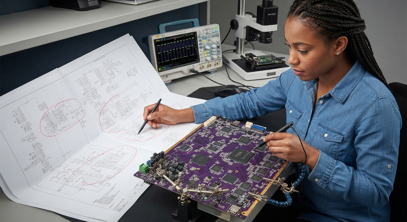
Ultimately, printed circuit board reverse engineering assemble faulty should be treated as a traceable engineering problem rather than simply an assembly failure. A reliable correction process moves backward from the faulty assembled PCB to the solder joints, component placement, PCB fabrication data, Gerber file, CAD file, layout drawing, and finally the original PCB. By systematically checking each stage, engineers can determine whether the problem comes from assembly, manufacturing, or an error in PCB reverse engineering. Once the root cause is confirmed, the design can be corrected, reproduced, and validated through a new prototype before entering further production.
Tags: pcb assemble reverse engineering,pcb board reverse engineering,pcb card reverse engineering,pcb reverse engineering,pcba reverse engineering,Printed Circuit Board Reverse Engineering,printed wiring board reverse engineering,pwb reverse engineering,pwba reverse engineering