

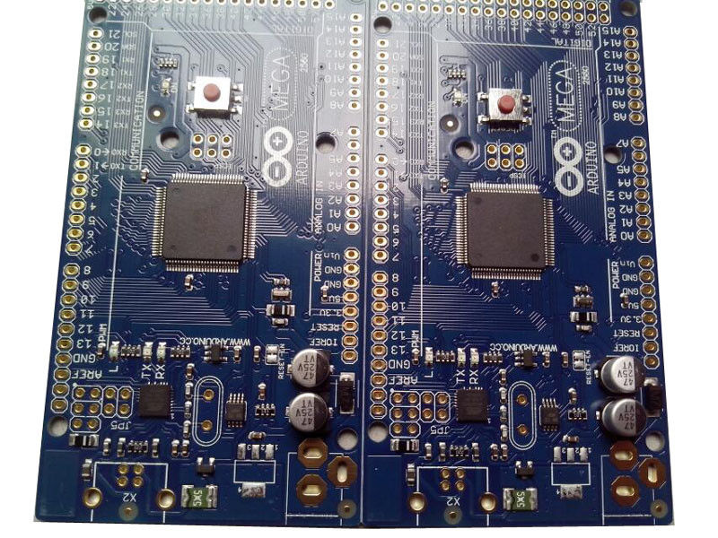
Reverse Engineering PCB Card
Reverse Engineering PCB Card can extract the layout, gerber file and schematic diagram from physical printed circuit board, these documents can be used to re-produce the new ones for PCB card cloning;
In the process of Reverse engineering PCB board schematic diagram, all of the electronic engineers and designers are all bearing the consciouceness of the root cause of noise generation among the power supply line and ground line, hereby describe the way of depress the noise.
As we all know add a decoupling capacitor among the power supply and ground line; furthermore, increase the size of power supply line and ground line, better to design the ground line wider than power supply line, their relationships is ground line wider than power supply line and wider than signal line, the signal line is 0.2 to 0.3mm, the thinnest circuit wide is 0.05 to 0.07mm, the power supply line is 1.2 to 2.5mm; as for the digital circuit, PCB card can use a relative wider ground line to form the loop, which can help to form a ground network. It is not applicable for the analog circuit.
Layout large area of copper foil on the PCB card, engineer should design other places where haven’t been used in the circuit pattern as ground line or produce it as multilayer PCB card, power supply and ground line can count for one layer separately;
Circuit Engineering Co.,Ltd. offers complete product life cycle support for reverse engineering PCB in the Medical, Industrial, Automotive, and Public Safety market segments. Our electronics design and electronic manufacturing services (EMS) core focus is vital in the creation of durable products that require high reliability. These products perform exceptionally well in even the most challenging environments.
At Circuit Engineering Co.,Ltd, we value our eletronic design and reverse engineering customers and their unique needs and expectations. Our customer focus and dedication to unparalleled excellence in PCB design, clone and manufacturing, has resulted in proven success in the industry.
Personal relationships are important to us. Our Business Managers, identified to support key Circuit Engineering Co.,Ltd customers, strive to build long term global partnerships. Our commitment to support our customers is backed by our electronics manufacturing history and demonstrated growth over the past ten years.
The Circuit Engineering Co.,Ltd is proud to have engineering and manufacturing facilities to support our customers. Our innovative PCB Reverse Engineering Service processes are performed at six (6) worldwide locations. These facilities are optimized for Reverse Engineering PCB Card capabilities in:
Reverse Engineering PCB
Microcontroller Extraction
Component Procurement
PCB Card Manufacturing Prototypes
New Product Development
New Product Introduction (NPI)
Supply Chain Management
Contract Manufacturing
Complete System Assembly
Test Development
Repair and Reverse Logistics Services
With extensive electronics design and innovative manufacturing capabilities, Circuit Engineering Co.,Ltd is able to execute to the highest quality and reliability expectations in the Reverse Engineering PCB industry.
Tags: copier pcb bom,copier pcb design,copier pcb layout,copier pcb part list,copier pcb schematic,reverse engineering circuit board,reverse engineering circuit card,reverse engineering pcb,reverse engineering pcb assemble,reverse engineering pcb board,reverse engineering pcb card,reverse engineering pcba,reverse engineering printed circuit board,reverse engineering printed wiring board,reverse engineering pwb,reverse engineering pwba