"Everything we build starts with design engineering. CECL manufactured boards for one of our products. It went perfectly – a real success.It is really an high quality service they have provided to us!"
By Nile Smith from Sinotech Inc.
“We had several very old device with obsolete boards need to be replaced –through CECL professional service.We got what we needed, and we’ve been using the results of the work without any problem till now.”
By Richard Anderson from TWP system Inc.
"Guys from CECL manufacture PCBs we use in one of our products, a clinometer and we’ve never had a problem with anything. The boards come in, they work. And, their team is very responsive."
By Ken Camerlo from Hi-END ADV Inc.
You are here: Home > Reverse Engineering PCB > Reverse Engineering Multilayer PCB Layout to Confirm Power Supply Layer Design
Reverse Engineering Multilayer PCB Layout to Confirm Power Supply Layer Design
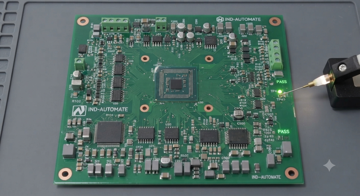
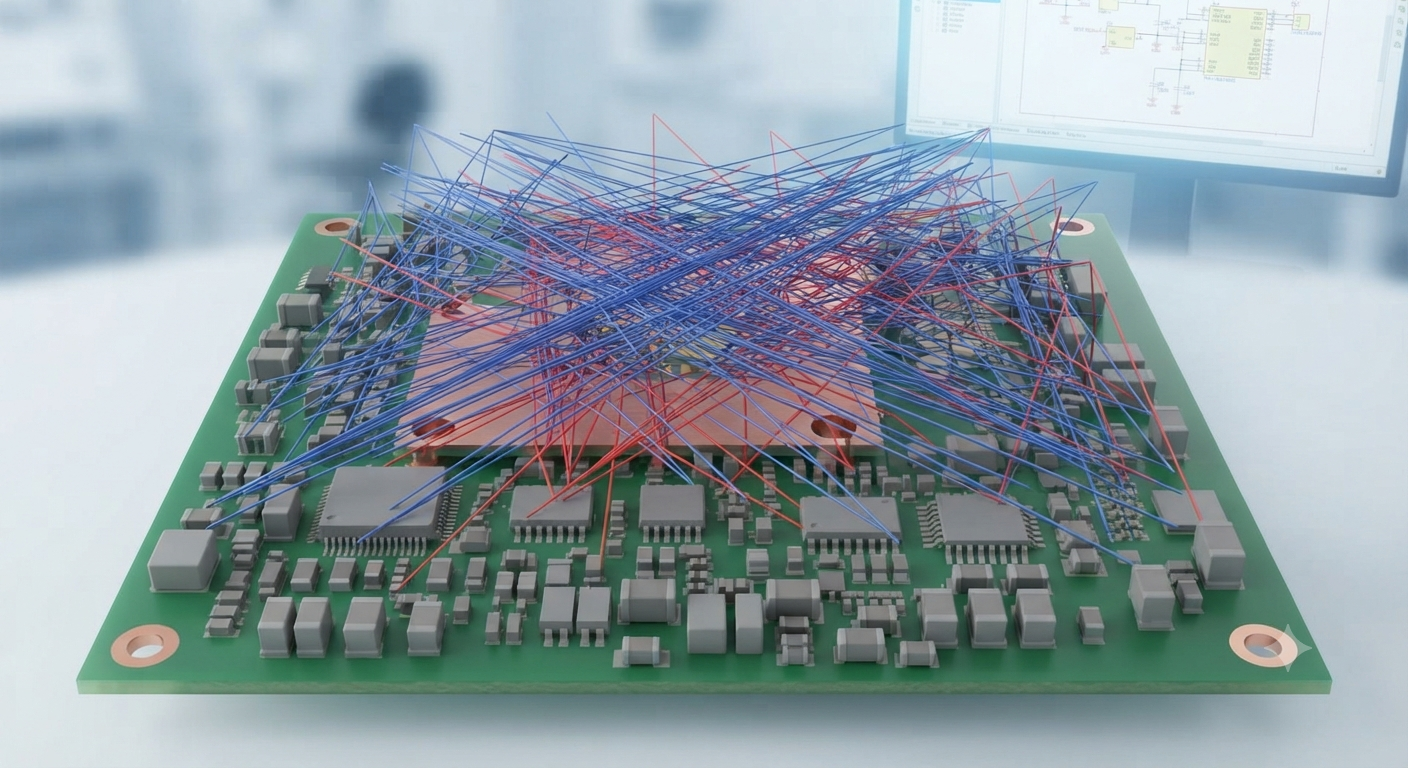
Inside complex industrial electronic control boards, stable power distribution is the backbone of reliable system performance. Multi-layer architecture allows modern controllers to separate sensitive signal traces from high-current power and ground planes, mitigating electromagnetic interference and voltage drops. However, when legacy hardware suffers from unexplained power faults, thermal throttling, or lack of official documentation, diagnosing the internal power supply layer becomes an extraordinary challenge. Performing targeted hardware analysis on multi-layer architecture is essential for uncovering hidden power planes, identifying design flaws, and restoring operational stability to critical industrial machinery.
Aby osiągnąć pełne zrozumienie wewnętrznej dystrybucji zasilania, wyspecjalizowane zespoły techniczne realizują zaawansowany proces extraction dostosowany do wytrzymałych konstrukcji wielowarstwowych. W celu skutecznego przeprowadzenia reverse engineering złożonej electronic circuit board lub industrial control unit, specjaliści wykorzystują precyzyjne skanowanie optyczne oraz sekwencyjne mechaniczne delayering, aby odsłonić ukryte warstwy zasilania i wewnętrzne warstwy ścieżek. Po tym dokładnym demontażu fizycznym eksperci mapują połączenia elektryczne w celu stworzenia funkcjonalnego netlist oraz precyzyjnego schematic diagram. Następnie specjaliści przygotowują kompleksową bom list, szczegółowe specyfikacje layout drawing, w pełni funkcjonalny cad file, dokładne gerber data oraz kompletny gerber file package. Wykorzystując te precyzyjne cyfrowe zasoby, zespoły inżynieryjne mogą skutecznie clone, replicate, duplicate, reproduce, restore, recovery, modify, remanufacture oraz prototype dowolną starszą printed circuit board, standard pcb board lub specjalistyczną pcb, tworząc w pełni zoptymalizowaną jednostkę zastępczą.
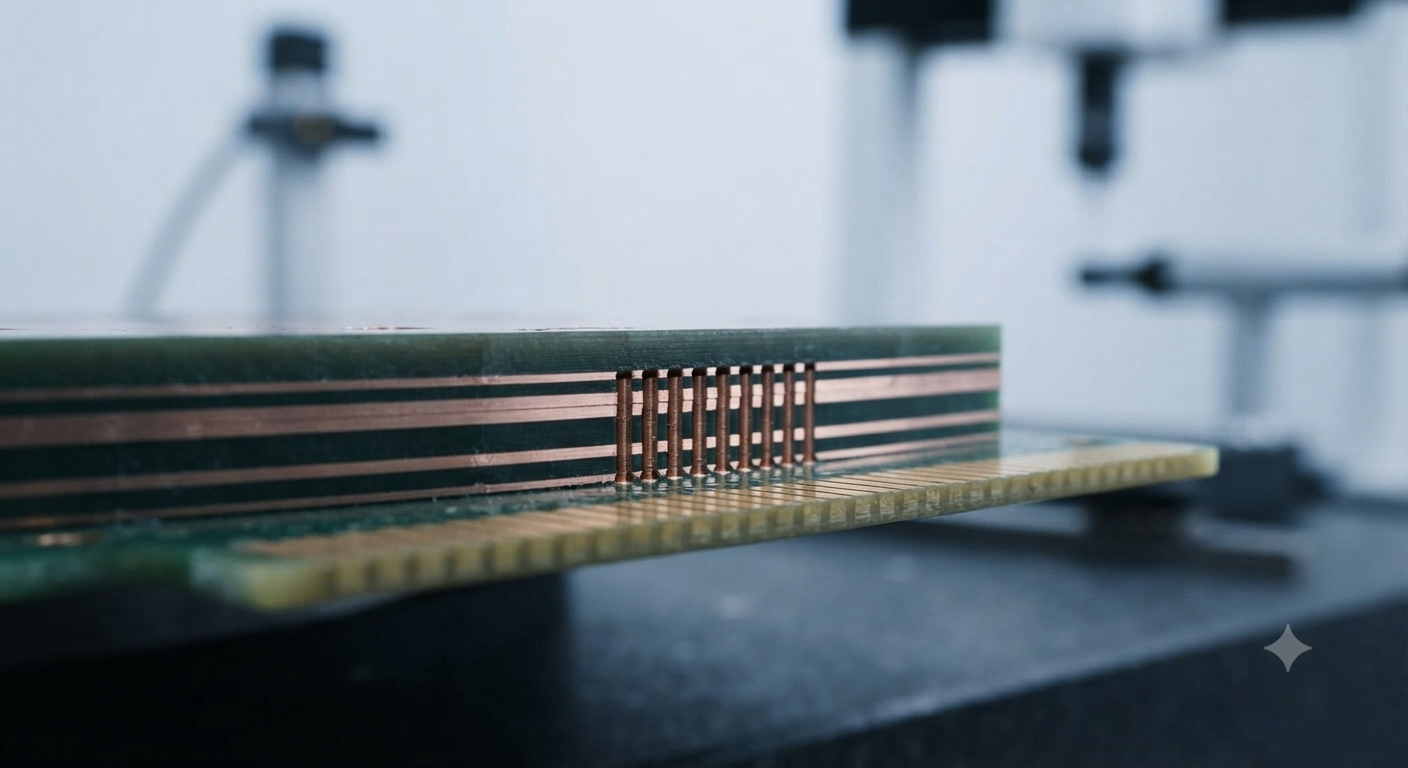
The primary hurdle in evaluating legacy power distribution networks lies in the opaque nature of multi-layer construction. Industrial controllers are engineered with buried copper planes that deliver clean voltage rails to microprocessors, gate drivers, and high-current actuators, completely hiding these critical pathways from exterior view. When troubleshooting external symptoms fails, technicians must look beyond surface inspections and systematically deconstruct the physical assembly. Unlocking the internal stacking arrangement ensures that engineers can accurately trace how power flows across the board, pinpoint voltage bottlenecks, and verify thermal dissipation integrity under heavy industrial loads.
Dahili güç dağıtım yapısını tamamen anlayabilmek için uzman teknik ekipler, dayanıklı çok katmanlı donanımlar için özel olarak tasarlanmış gelişmiş bir extraction süreci uygular. Karmaşık bir electronic circuit board veya industrial control unit üzerinde başarılı bir reverse engineering gerçekleştirmek için uzmanlar, gömülü güç katmanlarını ve iç iz katmanlarını ortaya çıkarmak amacıyla hassas optik tarama ve sıralı mekanik delayering tekniklerinden yararlanır. Bu ayrıntılı fiziksel incelemenin ardından uzmanlar, işlevsel bir netlist ve hassas bir schematic diagram oluşturmak için elektriksel bağlantıları haritalandırır. Daha sonra profesyoneller kapsamlı bir bom list, ayrıntılı layout drawing özellikleri, tamamen işlevsel bir cad file, doğru gerber data ve eksiksiz bir gerber file package hazırlar. Bu hassas dijital çıktılardan yararlanan mühendislik ekipleri, herhangi bir eski printed circuit board, standard pcb board veya özel pcb tasarımını etkili şekilde clone, replicate, duplicate, reproduce, restore, recovery, modify, remanufacture ve prototype ederek tamamen optimize edilmiş bir replacement unit oluşturabilir.
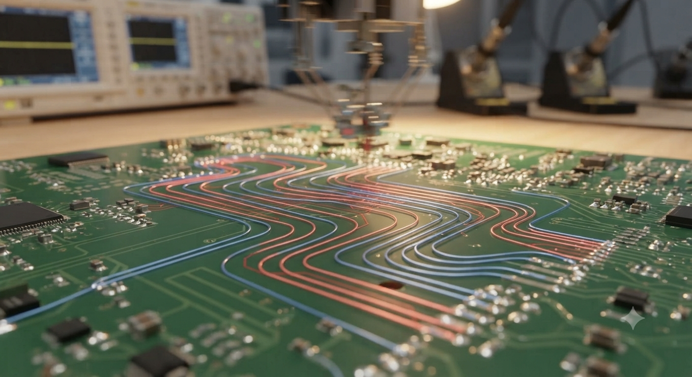
As for the high speed signal, this kind of unreasonable revert route design will bring severe security issue. As a result of that, high speed PCB board reverse engineering and layout should keep sufficient distance from power supply reference plane.
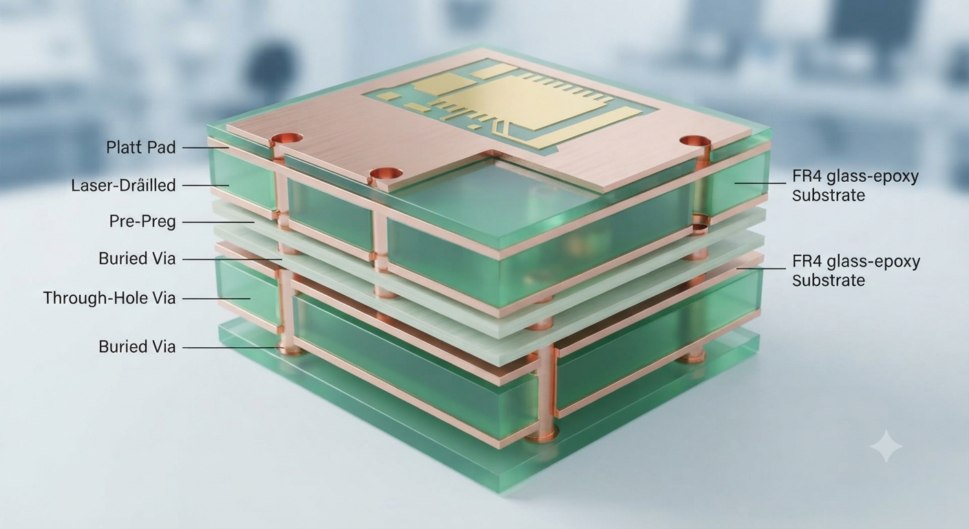
Multiple copper clad layer can effective decrease the impedance in the PCB and reduce the common mode electro-magnetic interference;
Signal layer should held close decoupling with adjacent reference plane and layers which means the inter-media thickness among the signal layers and adjacent copper layer should be keep as small as possible, and power supply copper clad should be close to ground copper clad as much as it can, as for this point, printed circuit board layout optimization can realize it.
Pentru a obține o înțelegere completă a distribuției interne de alimentare, echipele tehnice specializate execută un proces avansat de extraction adaptat pentru hardware industrial robust și structuri multi-strat. Pentru realizarea cu succes a unui reverse engineering asupra unei electronic circuit board complexe sau a unei industrial control unit, specialiștii utilizează scanare optică de precizie și procese mecanice secvențiale de delayering pentru a expune planurile interne de alimentare și straturile ascunse ale traseelor. După această analiză fizică detaliată, specialiștii cartografiază conexiunile electrice pentru a construi un netlist funcțional și un schematic diagram precis. Ulterior, profesioniștii compilează un bom list complet, specificații detaliate de layout drawing, un cad file complet funcțional, gerber data precise și un gerber file package integral. Folosind aceste livrabile digitale precise, echipele de inginerie pot efectua eficient clone, replicate, duplicate, reproduce, restore, recovery, modify, remanufacture și prototype pentru orice printed circuit board vechi, standard pcb board sau pcb specializat, transformându-le într-o unitate de înlocuire complet optimizată.
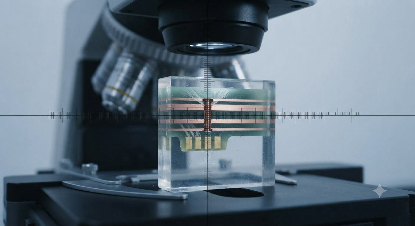
To achieve a complete understanding of internal power distribution, specialized technical teams execute an advanced extraction workflow tailored for rugged multi-layer hardware. To successfully reverse engineering a complex electronic circuit board or industrial control unit, experts utilize precision optical scanning and sequential mechanical delayering to expose buried power planes and inner trace layers. Following this meticulous physical teardown, specialists map the electrical pathways to build a functional netlist and a precise schematic diagram. From there, professionals compile a comprehensive bom list, detailed layout drawing specifications, a fully functional cad file, accurate gerber data, and a complete gerber file package. By leveraging these precise digital deliverables, expert engineering teams can effectively clone, replicate, duplicate, reproduce, restore, recovery, modify, remanufacture, and prototype any legacy printed circuit board, standard pcb board, or specialized pcb into a fully optimized replacement unit.
Pro dosažení úplného pochopení interní distribuce napájení provádějí specializované technické týmy pokročilý proces extraction přizpůsobený pro odolný vícevrstvý hardware. Pro úspěšné provedení reverse engineering složité electronic circuit board nebo industrial control unit využívají odborníci přesné optické skenování a postupný mechanický delayering k odhalení skrytých napájecích rovin a vnitřních vrstev spojů. Po této detailní fyzické analýze specialisté mapují elektrické propojení za účelem vytvoření funkčního netlist a přesného schematic diagram. Následně odborníci sestavují kompletní bom list, podrobné specifikace layout drawing, plně funkční cad file, přesná gerber data a kompletní gerber file package. Díky těmto přesným digitálním výstupům mohou inženýrské týmy efektivně clone, replicate, duplicate, reproduce, restore, recovery, modify, remanufacture a prototype jakoukoli starší printed circuit board, standardní pcb board nebo specializovanou pcb a vytvořit plně optimalizovanou náhradní jednotku.
Having a fully verified digital representation of the power supply layout empowers engineering teams to do much more than simply recreate the original hardware. Industrial environments change over time, and older power supply designs frequently suffer from inefficient copper weight distribution, thermal stress concentrations, or obsolete voltage regulators. With fully restored layout drawings and schematic files, maintenance personnel can safely modify or remanufacture the circuit board to incorporate modern, high-efficiency power components, improved decoupling networks, and robust thermal vias. This strategic upgrade path enhances overall electrical noise immunity and extends the lifespan of expensive machinery without requiring a wholesale system redesign.
PCB layout combination rationally: in order to complete the complicate layout on the PCB, it is inevitable to put the layer to layer switch into practice, and make the two layers cross by one signal route as layout PCB combination.
За постигане на пълно разбиране на вътрешното разпределение на захранването специализираните технически екипи изпълняват усъвършенстван процес на extraction, адаптиран за надежден многослоен хардуер. За успешно извършване на reverse engineering на сложна electronic circuit board или industrial control unit специалистите използват прецизно оптично сканиране и последователен механичен delayering процес за разкриване на скрити захранващи слоеве и вътрешни проводникови структури. След този подробен физически анализ експертите картографират електрическите връзки, за да създадат функционален netlist и точен schematic diagram. След това професионалистите подготвят цялостен bom list, подробни спецификации на layout drawing, напълно функционален cad file, точни gerber data и пълен gerber file package. Използвайки тези прецизни цифрови ресурси, инженерните екипи могат ефективно да clone, replicate, duplicate, reproduce, restore, recovery, modify, remanufacture и prototype всяка остаряла printed circuit board, стандартна pcb board или специализирана pcb, превръщайки я в напълно оптимизиран заместващ модул.
Switch among layers need to ensure the revert current can flow back from one reference plane to another. As a matter of fact, the best PCB reverse engineering layout combination is avoiding the revert current flow from one reference plane to another, from 3rd layer to 5th layer, from 5th layer to 7th layer, and then from 7th to 9th can be viewed as a layout combination.
But regards 3rd layer and 9th layer as a combination is not a reasonable option. Since it need to revert the current from 4th layer to decoupling 6th layer, and then from 6th layer to 8th layer which is not a smooth route for a revert current. Although can place the decoupling capacitor on around the through hole or decrease the medium thickness among the reference layer to reduce the ground bouncing.
Для полного понимания внутреннего распределения питания специализированные технические команды выполняют передовой процесс extraction, адаптированный для сложных многослойных аппаратных конструкций. Для успешного проведения reverse engineering сложной electronic circuit board или industrial control unit специалисты используют высокоточное оптическое сканирование и последовательный механический delayering, чтобы открыть скрытые силовые плоскости и внутренние слои проводников. После этого тщательного физического анализа специалисты создают карту электрических соединений для формирования функционального netlist и точного schematic diagram. Далее профессионалы составляют комплексный bom list, подробные спецификации layout drawing, полностью функциональный cad file, точные gerber data и полный gerber file package. Используя эти точные цифровые материалы, инженерные команды могут эффективно clone, replicate, duplicate, reproduce, restore, recovery, modify, remanufacture и prototype любую устаревшую printed circuit board, стандартную pcb board или специализированную pcb, превращая её в полностью оптимизированное сменное устройство.
Ultimately, mastering advanced power layer analysis transforms mysterious hardware failures into manageable, data-driven engineering solutions. By converting obscure multi-layer assemblies into pristine manufacturing documentation, businesses eliminate supply chain vulnerabilities and secure total control over their electronic maintenance assets. Ensuring that professional hardware recovery techniques are applied to power supply design guarantees that industrial electronic control boards will continue operating safely, efficiently, and reliably for decades to come.