"Everything we build starts with design engineering. CECL manufactured boards for one of our products. It went perfectly – a real success.It is really an high quality service they have provided to us!"
By Nile Smith from Sinotech Inc.
“We had several very old device with obsolete boards need to be replaced –through CECL professional service.We got what we needed, and we’ve been using the results of the work without any problem till now.”
By Richard Anderson from TWP system Inc.
"Guys from CECL manufacture PCBs we use in one of our products, a clinometer and we’ve never had a problem with anything. The boards come in, they work. And, their team is very responsive."
PCB Layout Drawing Reverse Engineering Test Methodology
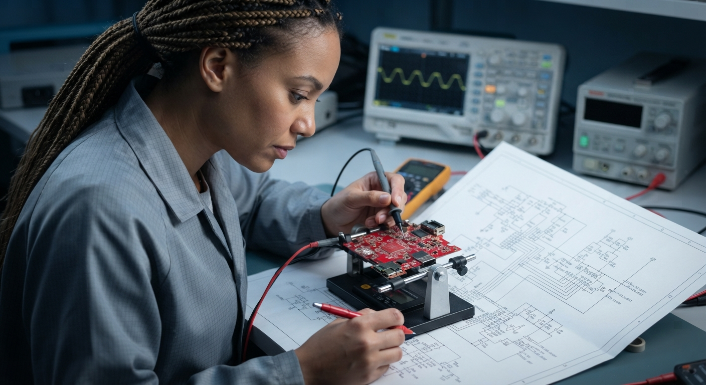
A strong PCB Layout Drawing Reverse Engineering Test Methodology should not stop at checking whether the recreated board looks similar to the original. The real objective is to verify whether the reverse-engineered engineering documents accurately describe the electrical and physical characteristics of the original PCB. A complete validation process normally covers the schematic diagram, PCB layout file, Gerber file, BOM list, and netlist.
Una solida metodologia di test per il reverse engineering del disegno del layout PCB non dovrebbe limitarsi a verificare se il circuito stampato ricreato appare simile all’originale. Il vero obiettivo è verificare se i documenti ingegneristici ottenuti tramite reverse engineering descrivono accuratamente le caratteristiche elettriche e fisiche della PCB originale. Un processo completo di validazione comprende normalmente lo schema elettrico, il file del layout PCB, il file Gerber, la lista BOM (Bill of Materials) e la netlist. Questi documenti sono interconnessi, quindi un errore in uno di essi può causare incoerenze negli altri. Ad esempio, un’impronta (footprint) errata di un componente nel file PCB potrebbe non essere evidente nello schema elettrico, ma potrebbe causare problemi durante l’assemblaggio. Pertanto, nella metodologia di test dovrebbero essere inclusi sia il confronto tra i diversi documenti sia la verifica della PCB originale rispetto alla relativa documentazione.
These documents are interconnected, so an error in one may cause inconsistencies in another. For example, an incorrect component footprint in the PCB file may not be obvious in the schematic diagram but can lead to assembly problems. Therefore, document-to-document comparison and original-board-to-document verification should both be included in the testing methodology.
The schematic diagram should first be checked against the physical PCB and the recovered netlist. Engineers can trace important signal paths from component pin to component pin and verify power, ground, communication, control, and analog circuits. Critical connections should be checked individually rather than relying only on automated electrical rules.
Una sólida metodología de prueba de ingeniería inversa del dibujo del diseño de una PCB no debería limitarse a comprobar si la placa de circuito impreso recreada tiene un aspecto similar al original. El verdadero objetivo es verificar si los documentos de ingeniería obtenidos mediante ingeniería inversa describen con precisión las características eléctricas y físicas de la PCB original. Un proceso completo de validación normalmente incluye el diagrama esquemático, el archivo de diseño de la PCB, el archivo Gerber, la lista BOM (Bill of Materials) y la netlist. Estos documentos están interconectados, por lo que un error en uno de ellos puede provocar inconsistencias en los demás. Por ejemplo, una huella de componente (footprint) incorrecta en el archivo de la PCB puede no ser evidente en el diagrama esquemático, pero puede provocar problemas durante el ensamblaje. Por lo tanto, la metodología de pruebas debe incluir tanto la comparación entre documentos como la verificación de la PCB original frente a la documentación correspondiente.
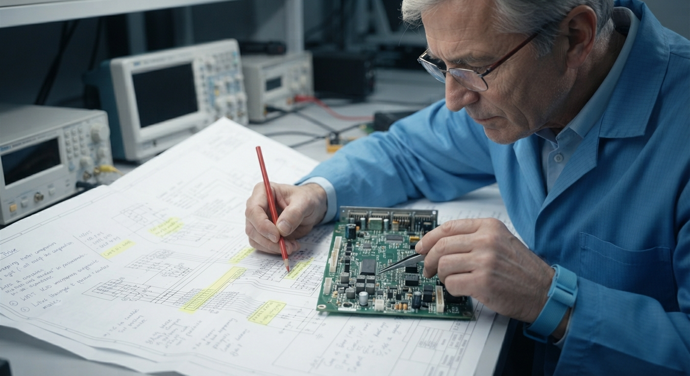
The BOM list should then be compared with the components physically installed on the original board, including reference designators, part numbers, package types, quantities, and component values. Special attention should be given to visually similar components and obsolete devices because an incorrect part number can result in different electrical characteristics. Cross-checking the BOM list, schematic diagram, and PCB file provides an effective way to identify inconsistencies before manufacturing a prototype.
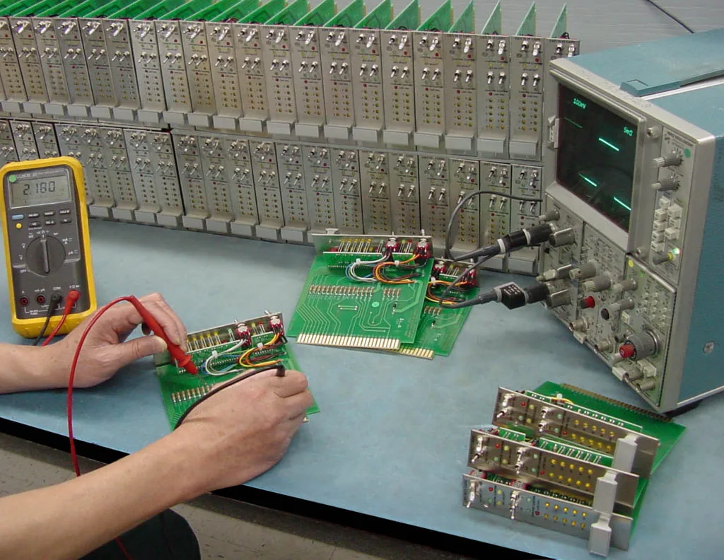
After PCB Layout Drawing Reverse Engineering, it is quite necessary to test its reliability and stability from physical and electrical features/properties.
By using the methodologies described herein, PWB Gerber file duplicating service suppliers and customers should expect to have significantly better correlation on the key PCB electrical parameters that affect high-speed digital bus designs.
With existing PCB card duplicating technology, the evolution of system bus design speed requires critical attention to design trade-offs for delivering high performance. These needs can be met by delivering strict PCB layout guidelines and rules that ensure requirements while utilizing low-cost FR4 dielectric PCBs. The combination of proper bus trace geometry and PCB test methodology are essential in understanding what existing PCB Reverse Engineering technology can deliver.
Uma sólida metodologia de teste de engenharia reversa do desenho do layout da PCB não deve se limitar a verificar se a placa de circuito impresso recriada é visualmente semelhante à original. O verdadeiro objetivo é verificar se os documentos de engenharia produzidos por meio da engenharia reversa descrevem com precisão as características elétricas e físicas da PCB original. Um processo completo de validação normalmente abrange o diagrama esquemático, o arquivo de layout da PCB, o arquivo Gerber, a lista BOM (Bill of Materials) e a netlist. Esses documentos são interconectados, portanto, um erro em um deles pode causar inconsistências nos demais. Por exemplo, um footprint incorreto de um componente no arquivo da PCB pode não ser evidente no diagrama esquemático, mas pode causar problemas durante a montagem. Portanto, tanto a comparação entre documentos quanto a verificação da PCB original em relação à documentação devem ser incluídas na metodologia de testes.
As PCB tolerances decrease, both proper coupon design and measurement procedures are essential for obtaining accurate results. This document presents recommendations for implementing test coupons and transmission line measurements to achieve with ±10% impedance variation.
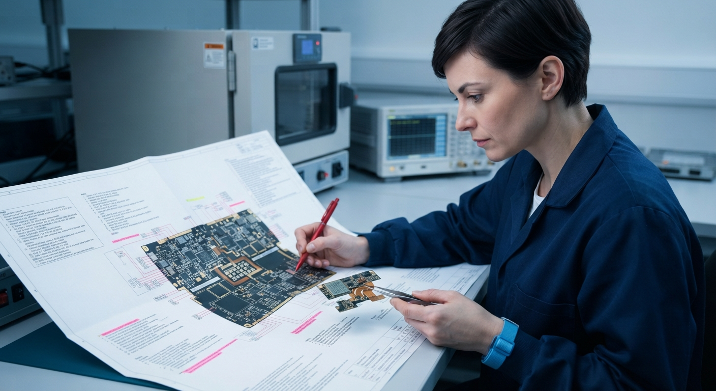
The PCB file and layout drawing require another level of verification. Engineers should compare component coordinates, footprints, pad dimensions, mounting holes, board outline, copper tracks, vias, and layer structures with the original PCB. For multilayer boards, internal copper routing should be validated using appropriate electrical measurements and layer-by-layer reconstruction techniques.
Une solide méthodologie de test de rétro-ingénierie du dessin de routage d’une PCB ne doit pas se limiter à vérifier si la carte de circuit imprimé recréée présente un aspect similaire à celui de l’originale. L’objectif réel est de vérifier si les documents d’ingénierie issus de la rétro-ingénierie décrivent avec précision les caractéristiques électriques et physiques de la PCB d’origine. Un processus complet de validation couvre normalement le schéma électrique, le fichier de routage de la PCB, le fichier Gerber, la nomenclature BOM (Bill of Materials) et la netlist. Ces documents sont interconnectés ; une erreur dans l’un d’eux peut donc entraîner des incohérences dans les autres. Par exemple, une empreinte (footprint) incorrecte d’un composant dans le fichier PCB peut ne pas être évidente sur le schéma électrique, mais elle peut provoquer des problèmes lors de l’assemblage. Par conséquent, la méthodologie de test doit inclure à la fois la comparaison entre les différents documents et la vérification de la PCB originale par rapport aux documents correspondants.
The resulting PCB file can also undergo design-rule checking to identify clearance violations, unconnected nets, short circuits, and other potential design problems. After this stage, the Gerber file should be generated from the verified PCB design and inspected independently. Engineers can use Gerber viewers to check copper layers, solder masks, silkscreens, drill files, and board outlines. Comparing these manufacturing layers with the original PCB provides an additional opportunity to discover incorrect routing or missing features before fabrication.
Een sterke testmethodologie voor reverse engineering van een PCB-layouttekening moet verder gaan dan alleen controleren of de gereconstrueerde printplaat er vergelijkbaar uitziet met het origineel. Het werkelijke doel is om te verifiëren of de door middel van reverse engineering gereconstrueerde engineeringdocumenten de elektrische en fysieke eigenschappen van de oorspronkelijke PCB nauwkeurig beschrijven. Een volledig validatieproces omvat normaal gesproken het schema (schematic diagram), het PCB-layoutbestand, het Gerber-bestand, de BOM-lijst (Bill of Materials) en de netlist. Deze documenten zijn onderling met elkaar verbonden, waardoor een fout in één document inconsistenties in andere documenten kan veroorzaken. Zo is een onjuiste component-footprint in het PCB-bestand mogelijk niet direct zichtbaar in het schema, maar kan deze tijdens de assemblage tot problemen leiden. Daarom moeten zowel document-tot-documentvergelijkingen als verificatie van de oorspronkelijke PCB ten opzichte van de bijbehorende documentatie in de testmethodologie worden opgenomen.
The final stage is prototype and functional verification. A small number of prototype PCBs can be manufactured from the validated Gerber file and assembled according to the recovered BOM list. Physical dimensions, component placement, electrical continuity, resistance values, power consumption, and important signal characteristics can then be compared with the original PCB. Functional testing under equivalent operating conditions provides the strongest confirmation that the reverse-engineered documentation is accurate.
Ideally, discrepancies should be recorded in a structured test report, traced back to the relevant schematic, PCB file, Gerber layer, BOM entry, or netlist connection, and corrected before another prototype is produced. In this way, PCB Layout Drawing Reverse Engineering Test Methodology becomes a controlled verification cycle rather than a simple visual copying process, significantly improving the accuracy and preciseness of the final engineering documentation.
Eine zuverlässige Testmethodik für das Reverse Engineering einer PCB-Layoutzeichnung sollte sich nicht darauf beschränken zu prüfen, ob die rekonstruierte Leiterplatte äußerlich der Originalplatine ähnelt. Das eigentliche Ziel besteht darin zu überprüfen, ob die durch Reverse Engineering erstellten technischen Unterlagen die elektrischen und physischen Eigenschaften der ursprünglichen PCB präzise beschreiben. Ein vollständiger Validierungsprozess umfasst normalerweise den Schaltplan, die PCB-Layoutdatei, die Gerber-Datei, die BOM-Liste (Bill of Materials) und die Netzliste (Netlist). Diese Dokumente sind miteinander verknüpft, sodass ein Fehler in einem Dokument zu Inkonsistenzen in anderen Dokumenten führen kann. Beispielsweise ist ein falscher Bauteil-Footprint in der PCB-Datei im Schaltplan möglicherweise nicht offensichtlich, kann jedoch zu Problemen bei der Montage führen. Daher sollten sowohl der Vergleich zwischen den einzelnen Dokumenten als auch die Überprüfung der Original-PCB anhand der zugehörigen Dokumentation Bestandteil der Testmethodik sein.