

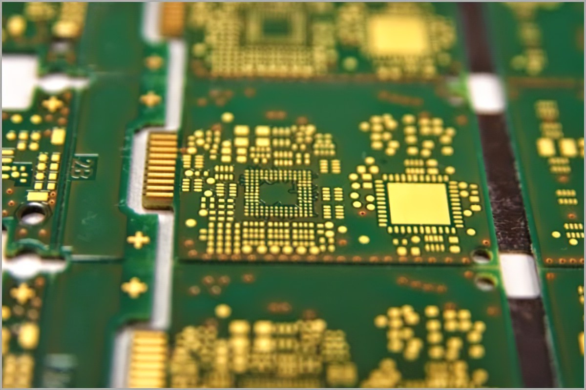
Reverse Engineering Multilayer PCB Board Schematic Diagram
Reverse Engineering Multilayer PCB Board Schematic Diagram needs to confirm the multiple power reference plane, multiple grounding reference planes;
The multi-power supply reference plane will be divided into several solid areas with different voltages. If the signal layer is in close proximity to the multi-power supply layer, the signal current on the adjacent signal layer will encounter an unsatisfactory return path, causing gaps in the signal return path.
For high-speed digital signals in the PCB board, this unreasonable return path design from Reverse Engineering Multilayer PCB Board Schematic Diagram may cause serious problems, so it is required that the high-speed digital signal routing should be kept away from the multi-supply reference plane.
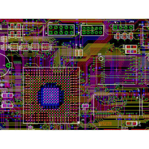
Multiple ground reference planes (ground planes) can provide a good low-impedance current return path that reduces common-mode EMl. Ground and power planes should be tightly coupled, and signal layers should be tightly coupled with adjacent reference planes. This can be achieved by reducing the thickness of the dielectric between layers;
Tags: Diagrama esquemático de la placa base multicapa de ingeniería inversa,Diagrama esquemático de placa de circuito multicapa de ingeniería inversa,Diagrama esquemático de placa electrónica multicapa de ingeniería inversa,Diagrama esquemático de placa PCB multicapa de ingeniería inversa