

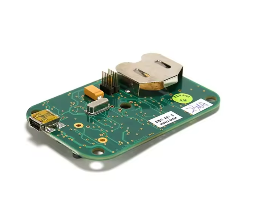
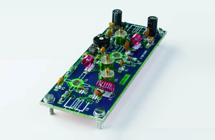
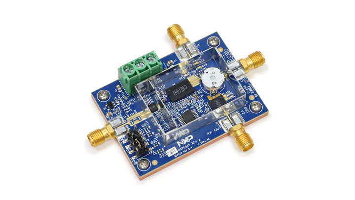
GSM Signal Amplifier Printed Wiring Board Replicate
In the fast-evolving field of wireless communications, GSM signal amplifiers play an essential role in boosting cellular coverage and ensuring reliable connectivity. At the heart of every amplifier lies a sophisticated Printed Wiring Board (PWB) that integrates RF circuits, filters, and power management modules. When the original documentation is missing, obsolete, or incomplete, companies often turn to GSM Signal Amplifier Printed Wiring Board Replicate services. This process, driven by reverse engineering, allows engineers to recover, restore, and recreate the critical technical data necessary to reproduce or remanufacture functional boards.
The Process of Reverse Engineering a GSM Signal Amplifier PCB
The replication of a GSM amplifier PWB begins with a detailed analysis of the existing hardware. Engineers examine physical layers, map copper traces, and document signal pathways. Using advanced imaging and CAD tools, they generate new Gerber files, schematic diagrams, layout drawings, BOM lists, and netlists. Each of these outputs serves a unique function in the replication process:
- Gerber file – Encodes the copper trace geometry, solder mask, and silkscreen layers. Accurate Gerber files ensure the amplifier board can be faithfully reproduced without missing or shorted signal paths.
- Schematic diagram – Shows the logical circuit design of amplifiers, filters, and power regulation. The schematic allows technicians to redesign or redevelop circuits if performance enhancements are required.
- Layout drawing – Defines the precise mechanical placement of RF components, grounding planes, and connectors, all critical for maintaining signal integrity at GSM frequencies.
- BOM list – Provides a complete inventory of parts, including RF transistors, inductors, capacitors, and shielding components. This document ensures compatibility when sourcing or refurbishing assemblies.
- Netlist – Maps pin-to-pin electrical connectivity, enabling verification that every signal is routed correctly before mass production.
GSM Signal Amplifier Printed Wiring Board Replicate needs to firstly extract the PCB circuit board’s gerber file and schematic diagram, then reproduce the GSM Signal Amplifier card by these documents;
After you get started of your GSM Signal Amplifier PCB Reverse Engineering, all the necessary files will be submited in below format through which your printed wiring board can be manufacture and assembly anywhere in the world, we can ensure the accuracy of your data by means of prototype running.
Value of Technical Document Recreation
Through reverse engineering, these documents are not just copies of the original—they often provide opportunities for duplication, cloning, or even redesign with modern components. For example, obsolete RF transistors may be substituted with more efficient models, improving overall amplifier performance. Similarly, layout refinements can reduce electromagnetic interference (EMI) and enhance durability under harsh environmental conditions.
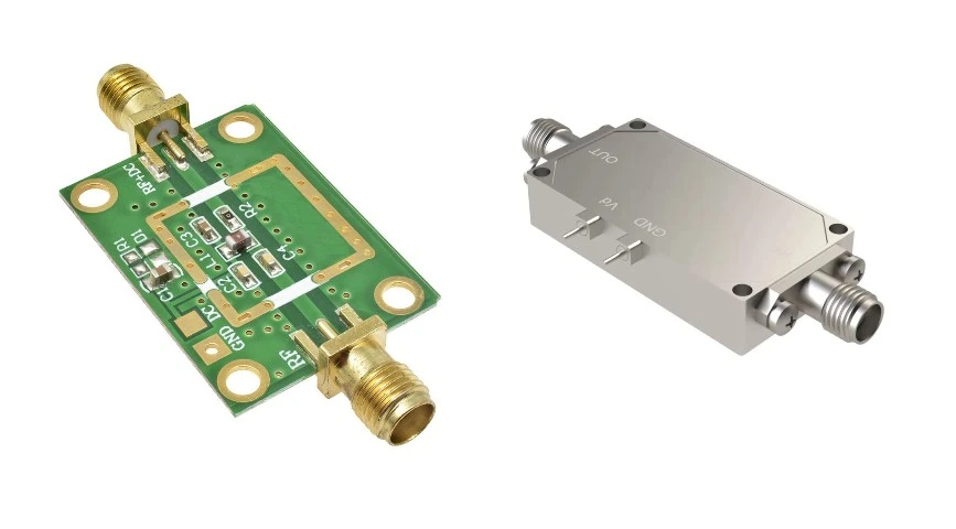
Applications in the Wireless Communication Industry
The ability to replicate GSM signal amplifier PWBs carries immense value across the wireless sector. Network providers may need remanufactured boards to extend the service life of legacy infrastructure, particularly in regions where GSM remains the backbone of connectivity. Repair facilities benefit from the ability to restore discontinued amplifier models, ensuring continued service without depending on OEM supply chains. Manufacturers, meanwhile, can use the recreated technical data for redevelopment, integrating GSM amplification into hybrid systems that also support LTE or 5G technologies.
Here is sample of files and drawings you will receive, based on a typical double layer GSM Signal Amplifier PCB board cloning with components mounted on two sides:
BOTTOM layer of Gerber File from GSM Signal Amplifier:

TOP layer of Gerber File from GSM Signal Amplifier:

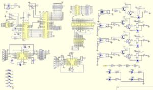
SCHEMATIC diagram from GSM Signal Amplifier:

The process of GSM Signal Amplifier Printed Wiring Board Replicate is more than a technical exercise—it is a bridge between past and future communication systems. By generating validated Gerber files, schematic diagrams, layout drawings, BOM lists, and netlists, reverse engineering empowers companies to recover, duplicate, and redesign amplifier boards that remain vital to the wireless ecosystem. Whether for maintenance, refurbishment, or innovation, this service ensures that GSM networks continue to provide reliable connectivity worldwide.
Circuit Engineering Company Limited provide a complete PCB Reverse Engineering, PCB Clone and PCB Restoration service, Rapid Prototyping and functional test services using the latest technologies combined with traditional skills for a wide range of industries. By integrating our traditional skills with the latest technologies, we can offer clients a comprehensive portfolio of product development services all under one roof. For more details please contact our customer service team.
Tags: rigid flex printed wiring board replicate,single side printed wiring board replicate