

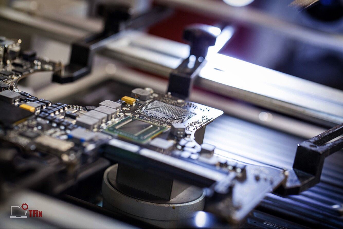
High Speed PCB Wiring Card Cloning Integration
Accompany with the development of High Speed PCB Wiring Card Cloning Integration technology and the decreasing of the PCB wiring card dimension, the circuit functions is growing, as well as the time clock speed and component rising speed have all been promoted, high speed design has already become a very important part in the whole PCB Wiring card Cloning process.
In order to deal with the more and more popular high speed issue in the Pcb wiring card Cloning, it is very important to take the signal analysis as basis, combine with the swift verification in the end stage of design to fulfill a comprehensive design method.
Most of the design engineers are all familiar with the reliability issue in the high speed circuit design, and the way to tackle the reliability issue is still base upon the experience, and few of the high speed analysis should be combined into the design. However the high speed PCB Wiring card Cloning has already became the un-avoidable and un-evitable issue in the whole process, systematic clock in the Ghz level, high speed systematic data-bus, less and less physical dimension, especially the components is lower than the nano rank rising time, which will make even the most universal pcb wiring card will have the signal integrity issue.
Nowadays, PCB Wiring Card Cloning has become more and more difficult, with daily increasing design complexity and smaller size of components with thin footprint from PCB Wiring Card Cloning will make the density of circuitry more intense, which will cause the transmission line effect and other signal integrity issue become more common.

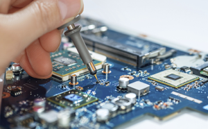
For example, simply increase the semiconductor climbing time after PCB Wiring Card Cloning and introduce the cross talk and alarm clock vibration phenomenon in the already finished PCB board layout drawing and Gerber file. and designer is becoming more and more concerned about the reliability of the project, so they are going to need to use the schematic diagram to inspect the correctiveness of the PCB layout drawing acquired from PCB reverse engineering.