PLC Board Reverse Engineering: Reading Opto-Isolation and Backplane Buses

A PLC rack rarely fails all at once. It fails one card at a time — an eight-channel digital input module here, a four-channel analogue card there — and the spare that once arrived within a week has been discontinued. When the vendor’s catalogue closes that door, PCB reverse engineering becomes the practical route back. Programmable logic controllers are a good place to begin a series on industrial PCB reverse engineering, because nearly every difficulty found elsewhere in industrial electronics appears, in miniature, inside a single I/O card.
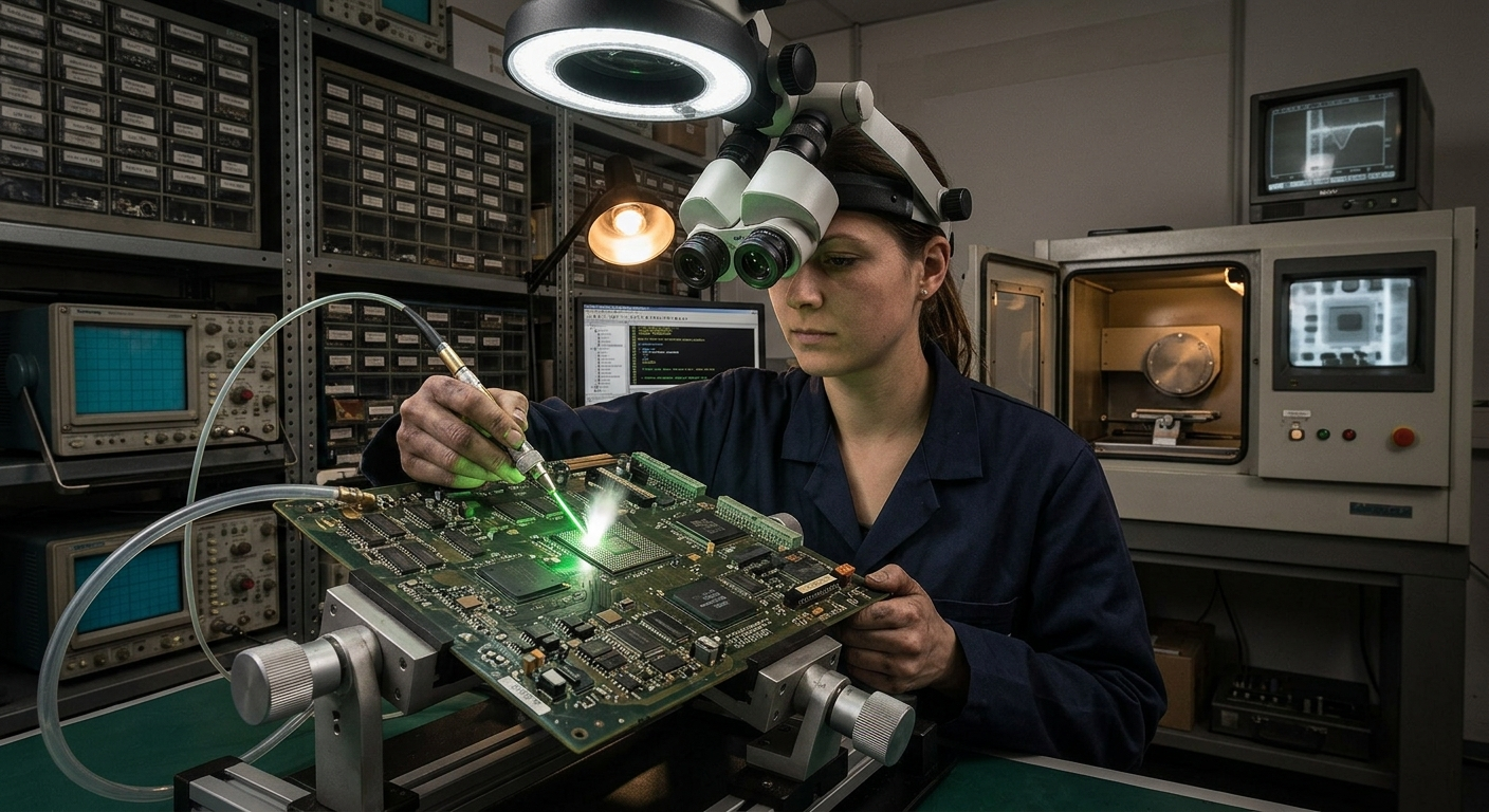
PLC donanımının PCB tersine mühendisliğinde en yaygın hatalardan biri, kartın kendi başına çalışan bağımsız bir yapı olduğunu düşünmektir. Aslında durum böyle değildir. Arka panel (backplane), her yuva tarafından paylaşılan adres hatlarını, veri hatlarını, chip select ve el sıkışma sinyallerini taşır ve kartın davranışı bu sinyallerin nasıl çözümlendiğine bağlıdır. Chip-select pini bağlantısız görünen bir kart genellikle CPU modülündeki decode mantığına dayanır. Bir PLC devre kartı kurtarma projesi, bus arayüzünü açık şekilde dokümante etmelidir: sinyal adlandırmaları, bus transceiver bileşenleri, seri sonlandırma, her kart için address decode yapısı ve slot tanımlama bağlantıları dahil edilmelidir. Tek bir kartı doğru şekilde analiz etmek, tüm sistemin doğru şekilde çözümlendiği anlamına gelmez.

What is actually inside an I/O module

Every input or output card is built from three functional blocks, and the boundaries between them define how the board should be read:

  1. The field interface. Terminals, transient suppression, current limiting and reverse-polarity protection.
  2. The isolation barrier. Optocouplers or digital isolators for discrete channels; isolated amplifiers or transformer coupling for analogue ones.
  3. The logic and backplane side. Shift registers, analogue multiplexers, a small CPLD and the bus transceivers.

Reading the card as three blocks, not one dense netlist, is the first decision in any PLC board reverse engineering project.

Reading the two signal paths

Digital channels — the opto-isolation path

A discrete input channel looks trivial on paper: a series resistor, a protection diode and an optocoupler LED. In practice those three parts carry all of the engineering. The series resistor sets forward current at nominal field voltage; the protection diode clamps reverse transients; the LED’s current transfer ratio and the phototransistor pull-up fix the switching threshold. Recover the wrong resistor value, and the card may pass a bench test at 24 V while failing in the field at 19 V.
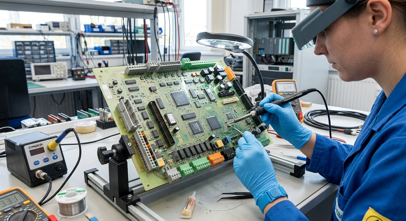
Найпоширенішою помилкою під час зворотного проєктування PCB обладнання PLC є розгляд плати як повністю автономного модуля. Насправді це не так. Об’єднавча плата (backplane) передає адресні лінії, лінії даних, сигнали chip select і сигнали handshake, які спільно використовуються всіма слотами, а поведінка плати залежить від того, як ці сигнали декодуються. Плата, у якої контакт chip-select виглядає непідключеним, зазвичай використовує логіку декодування в модулі CPU. Проєкт відновлення плати PLC повинен чітко документувати інтерфейс bus: найменування сигналів, трансивери bus, послідовну термінацію, декодування адрес для кожної плати та будь-які перемички або налаштування ідентифікації слота. Правильний аналіз однієї плати не означає правильне відновлення всієї системи.

Three parameters must be captured:

  • Input current and threshold. Measured with the board powered, not inferred from the schematic shape.
  • Filter constants. The RC network or digital debounce that stops contact chatter reaching the bus.
  • Isolation geometry. Creepage and clearance across the barrier, as much a part of the design as any value.

Analogue channels — multiplexing and scaling

Analogue cards are harder: the error budget is set by networks that cannot be read by eye. A typical layout is a divider or instrumentation amplifier per channel, an analogue multiplexer such as a 4051 or 4053, a shared ADC and a reference. Each channel’s RC filter feeds the multiplexer, and the multiplexer’s on-resistance interacts with it, so tolerances matter twice over.

The elements worth recovering first are:

  • the reference voltage, which fixes the absolute scale;
  • the gain network, which fixes the span;
  • the multiplexer control lines, which reveal the channel addressing order;
  • the isolation topology, which distinguishes linear optocoupler feedback from PWM modulation.

Without these, a recovered schematic is electrically correct but numerically meaningless — where schematic recovery stops being a drawing exercise and becomes a measurement problem.
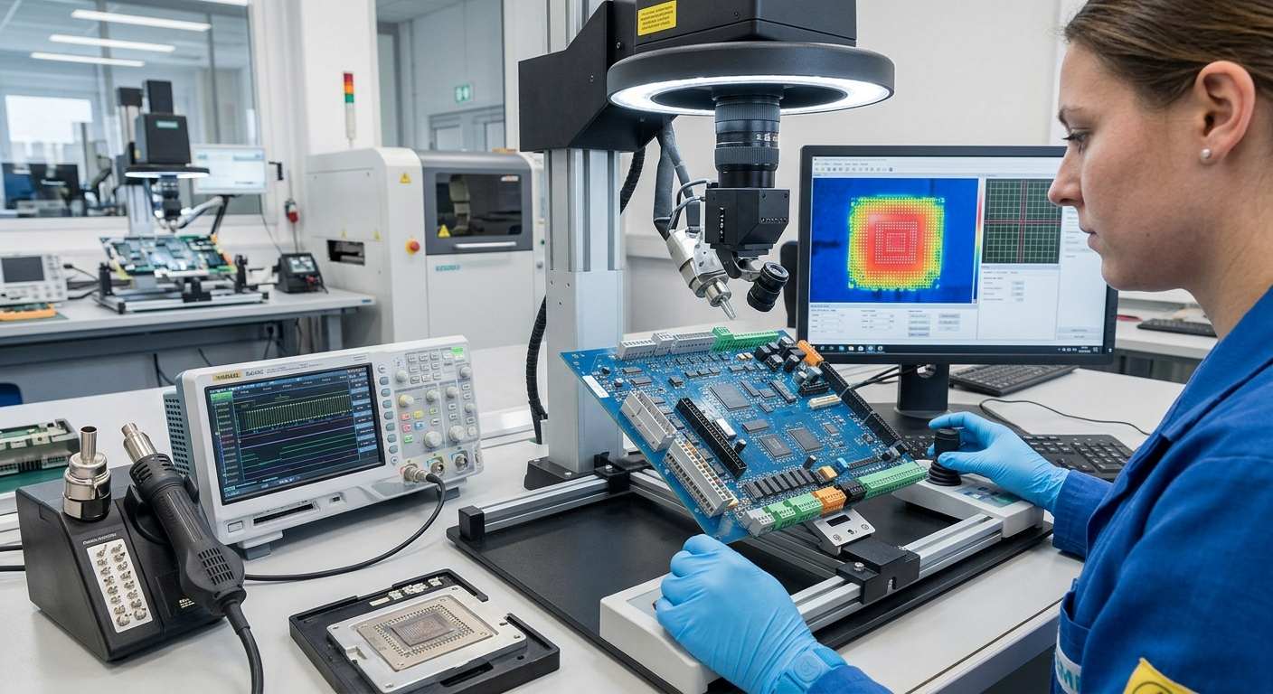
PLC हार्डवेयर की PCB रिवर्स इंजीनियरिंग में सबसे सामान्य गलती यह मानना है कि कार्ड एक स्वतंत्र और स्वयं-पूर्ण इकाई है। वास्तव में ऐसा नहीं होता। बैकप्लेन (backplane) सभी स्लॉट द्वारा साझा की जाने वाली address lines, data lines, chip select और handshake signals को वहन करता है, और कार्ड का व्यवहार इस बात पर निर्भर करता है कि इन संकेतों को किस प्रकार decode किया जाता है। जिस कार्ड का chip-select pin जुड़ा हुआ दिखाई नहीं देता, वह सामान्यतः CPU module में मौजूद decode logic पर निर्भर करता है। PLC circuit board recovery project में bus interface को स्पष्ट रूप से दस्तावेज़ करना चाहिए, जिसमें signal naming, bus transceivers, series termination, प्रत्येक कार्ड के लिए address decode और slot identification strapping शामिल हों। एक कार्ड का सही विश्लेषण करना पूरे सिस्टम को सही रूप से समझने के समान नहीं है।

The backplane bus is where mistakes hide

The most common error in PCB reverse engineering of PLC hardware is treating the card as self-contained. It is not. The backplane carries address lines, data lines, chip selects and handshake signals shared by every slot, and the card’s behaviour depends on how it decodes them. A card whose chip-select pin appears unconnected usually relies on decode logic in the CPU module.

A recovery project should document the bus interface explicitly: signal naming, bus transceivers, series termination, address decode per card and any slot-identification strapping. Getting one card right is not the same as getting the system right.

A practical recovery sequence

Order of operations matters more than technique. Most industrial jobs follow the same reverse engineering workflow:

  1. Document before touching anything. High-resolution photographs of both sides, revision numbers, date codes and any conformal coating.
  2. Map mechanically. Record every pad, via and mounting feature, then image the copper layers or de-layer selectively.
  3. Extract the netlist layer by layer, checking inner-layer traces against the outer ones.
  4. Rebuild the schematic and resolve ambiguous nets by continuity measurement rather than assumption.
  5. Cross-check against a working card, powering the board and measuring the parameters identified above.

Steps three and four carry most of the accuracy: a netlist error on an inner layer propagates silently into the schematic and into any board made from it.
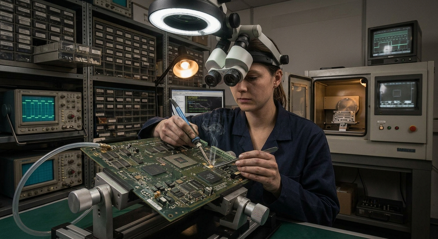
Najczęstszym błędem podczas inżynierii odwrotnej PCB sprzętu PLC jest traktowanie karty jako niezależnego, samodzielnego modułu. Tak jednak nie jest. Płyta tylna (backplane) przenosi linie adresowe, linie danych, sygnały chip select oraz sygnały handshake współdzielone przez wszystkie gniazda, a działanie karty zależy od sposobu ich dekodowania. Karta, której pin chip-select wygląda na niepodłączony, zazwyczaj wykorzystuje logikę dekodowania znajdującą się w module CPU. Projekt odzyskiwania płytki drukowanej PLC powinien dokładnie dokumentować interfejs bus: nazwy sygnałów, transceivery bus, terminację szeregową, dekodowanie adresów dla każdej karty oraz wszelkie połączenia identyfikacji slotu. Poprawne odtworzenie jednej karty nie oznacza jeszcze poprawnego odtworzenia całego systemu.

How this work is approached

This is the focus of our team at Circuit Engineering Company Limited: industrial circuit boards, recovered from the physical hardware, delivered as editable data the client owns. The output — netlist, schematic, fabrication data and a bill of materials with substitutes for obsolete parts — is what a plant needs to keep an old rack alive.

PLC I/O modules reward patience. They are small, yet compress the whole discipline into a few square centimetres: an isolation barrier with real safety constraints, analogue scaling that must be measured rather than guessed, and a bus interface that only makes sense in the context of the whole rack. Read them in that order and PCB reverse engineering stops looking opaque.