


PCB Reverse Engineering on Coated and Potted Boards
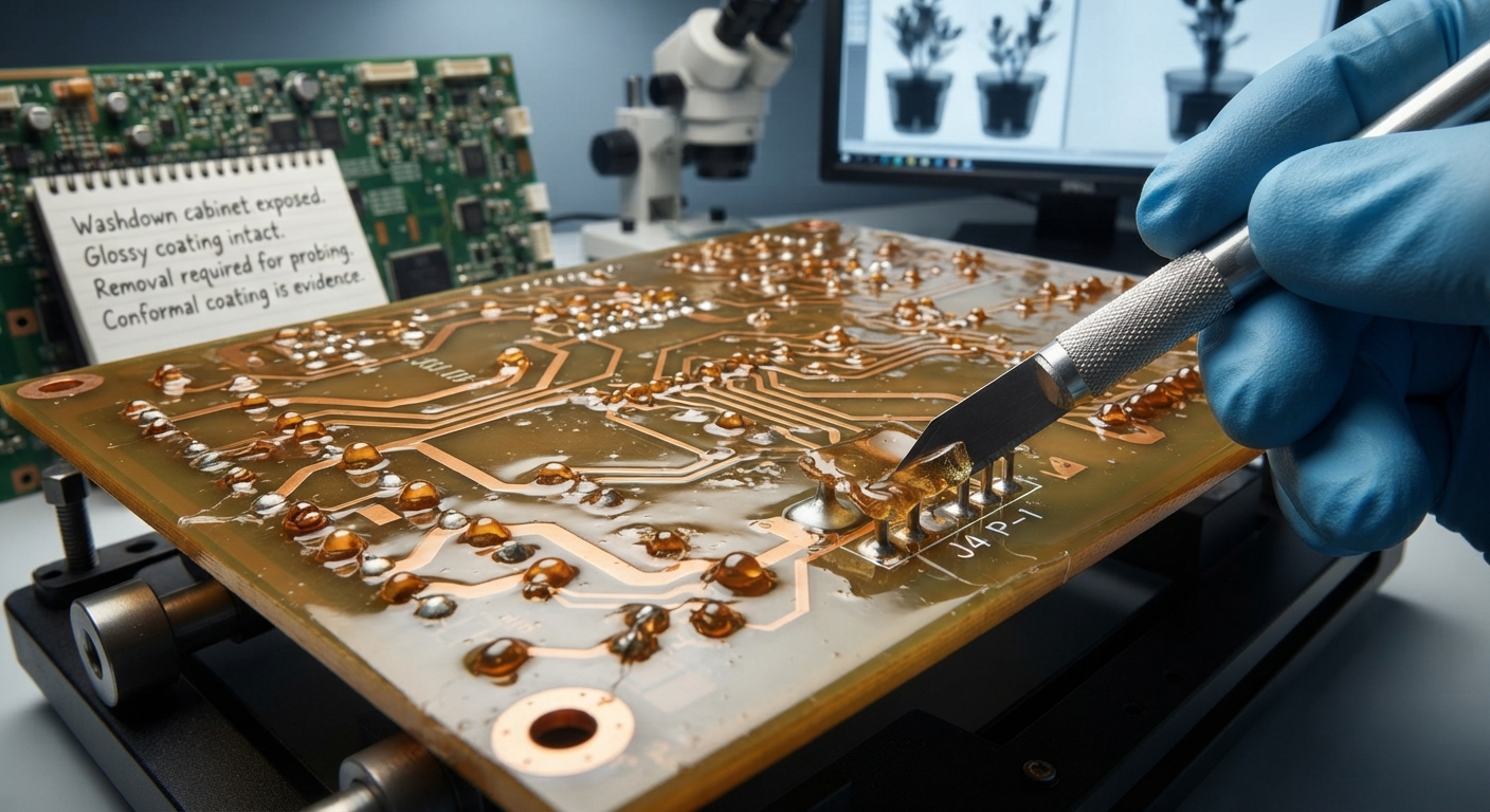
A board that has spent ten years inside a washdown cabinet arrives with a glossy skin over every joint. The reflex is to treat that skin as dirt and scrape it away. It is better treated as an information layer: the coating says what environment the board was built for, and it sets the order in which evidence can be collected. On coated and potted assemblies, PCB reverse engineering is a removal problem before it is an electrical one.
What the coating hides, and what it does not
Five chemistries cover most industrial boards, and each behaves differently under a knife and a solvent:
- Acrylic (AR) — thin, fluorescent blue-white under UV, dissolves readily in acetone or isopropyl alcohol.
- Polyurethane (UR) — tougher and more chemical-resistant; dedicated strippers swell it rather than dissolve it, and it tends to lift traces if pulled cold.
- Silicone (SR) — soft, peelable in sheets, but it creeps into connectors and under shield cans.
- Epoxy (ER) — two-part, near-permanent, common on potted power modules.
- Parylene (XY) — vacuum-deposited, micron-thin and pinhole-free, immune to solvents; only plasma or abrasion removes it.
What survives is useful: silkscreen is usually legible through a thin coat, laser-marked part numbers still read at 20×, and top-layer routing remains visible under oblique light because the coating follows the copper. What disappears is the cheap evidence — test pads, via annuli, the difference between a cold joint and a good one, and any hairline crack in a solder fillet.
Identify the coating before removing any of it
Start with a UV lamp in a dark room. Acrylic glows strongly, urethane faintly, parylene not at all. Then run a solvent spot test on a corner of scrap copper near a mounting hole — never beside a crystal, a connector or a membrane switch. Acetone handles acrylic in seconds; urethane needs a commercial stripper and twenty minutes; epoxy needs dichloromethane, which also attacks legends, connector bodies and some wire insulation.
Opening local windows
Mechanical removal beats blanket stripping on a board you cannot replace. A glass-brush in a dental handpiece cuts a controlled-depth window in seconds; laser ablation opens 0.2 mm windows over fine-pitch pads without touching neighbouring mask. Hot air plus a peel works on silicone. Aim for a window two or three millimetres wide over one measurement point, probe it, then re-seal before moving on.
Potted modules: what is still recoverable
Potting is a different problem. Filled epoxy is poured into a cavity, bonds to every component and cures hard, so there is no surface to peel. The recoverable information is volumetric: CT the intact brick first. Layer count, plane shapes, transformer and heatsink positions and the outline of the power stage usually come through, which is often enough to draft topology and to decide whether the rest is worth the risk.
Then cut, deliberately. Mill the base plate, dig from the side where compound is thinnest, or dissolve a small unit in methylene chloride over days. Expect casualties, and keep one sacrificial unit for exactly this. This is where PCB reverse engineering turns into a decision about acceptable loss.
The honest limits
A potted DC-DC brick sometimes stops at a functional model: input range, output rails, ripple, thermal derating, no netlist. That is a legitimate result. Claiming a full schematic from a filled module without destructive cross-sections is not.
A sequence that preserves evidence
Coating removal is irreversible, so in PCB reverse engineering the order of operations is the method:
- Photograph both sides under white light and UV before anything is touched.
- X-ray or CT the assembly intact; archive the volume data, not just the prints.
- Confirm the chemistry by UV response plus a solvent spot test on scrap copper.
- Open local windows over measurement points instead of stripping whole areas.
- Probe under a microscope, then re-seal each window before starting the next.
- Log solvent, dwell time and photographs against the board revision.
What coating removal changes downstream
The reproduction needs the coating callout as much as the copper. Record the material class, the masking map — connectors, test points, relay contacts, pressure sensors — and the cure schedule, because a legacy board reproduction that omits them will fail in the same cabinet the original survived. Where a potted module is replaced by a coated housing, write the deviation down.
Circuit Engineering Company Limited works on industrial boards — PLC racks, drive stages, switch-mode supplies — starting from the physical board and delivering editable data the client owns. Coating and potting evidence travels with the reverse engineering workflow as its own record set, and anything inferred rather than measured enters schematic recovery with a confidence note attached to the node.
Treat the coating as a document. Read it, sample it, open only what you must, and the board underneath gives up its netlist with its joints still intact.