

PCB Reverse Engineering Calibration
PCB Reverse Engineering Calibration against a standard is completed to determine the offset between instrument measured and actual PCB impedance. Complete this by following the average mean method described in the measurement section of this document extracted from Printed wiring board component arrangement. After determining the difference between the known standard value and the instrument reading, use this value as a fixed offset to obtain the actual PCB impedance.
Calibration against standard should be completed daily.
Example:
- · Calibrated standard
- · Measured value
- · Offset value (25 – 27)
= 25 Ω (±0.1)
= 27 Ω
= -2.0 Ω
Therefore, the measured values in this example will need to subtract 2 Ω to obtain the actual (real) PCB impedance. For this example a measured value of 33 Ω will correspond to an actual 31 Ω impedance. Again, for this example, the apparent measurement spec window for Direct Rambuswould be 27.2 Ω to 32.8 Ω in order to meet the actual 25.2 Ω to 30.8 Ω requirement.
Airline- 28 Ohm (Preferred)
Calibration against a 28 Ω, open-ended airline provides the most accurate calibration. This will require a custom-made airline. The primary disadvantages of air-lines are availability and cost from PCB card Reverse Engineering analysis.
- · Disconnect probe from cable, connect airline and measure.
- · Airline specifications:
28 Ω ±0.1DC to > 2 GHz
7 mm or 3.5 mm
15 cm min length
30 cm max length
NIST Certified
Airline- 25 Ohm
Calibration to 25 Ω can be completed by utilizing two commonly available 50 Ω, open-ended airlines connected in parallel as illustrated in Figure 5. Both airlines must be identical in electrical delay and model type. The disadvantage of the 25 Ω calibration is slightly reduced accuracy while having significant advantages with cost and availability.
- · Disconnect probe from cable, connect airlines and measure.
- · Airline specifications:
50 Ω ±0.1 DC to >2GHz
7 mm or 3.5 mm
SMA T 50 Ω (MACOM #2041-6204-00)
15 cm min length
30 cm max length
NIST Certified
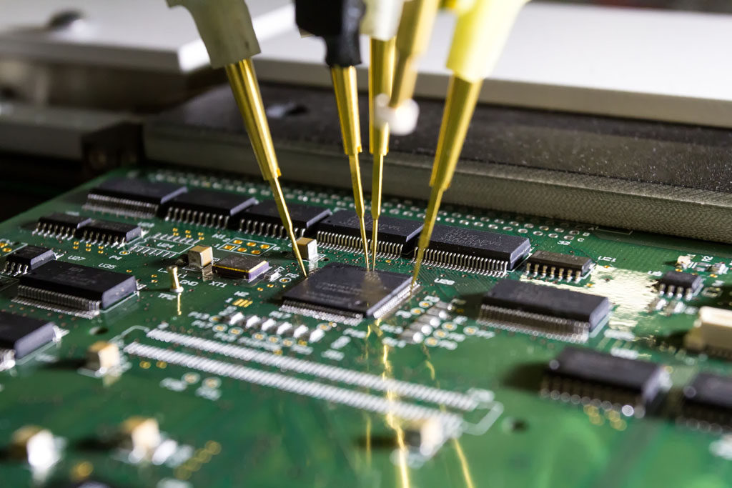
Probing Techniques
The most commonly used probe techniques in use today are handheld, SMA, and microprobe. The primary factors that need to be considered when choosing the probe technique that will be used are accuracy and the amount of work involved to complete the measurements. The difference between probes will play a critical role in accuracy, correlation and repeatability of PCB Reverse Engineering.
The probe’s purpose is to provide the medium for injecting the pulse from the TDR’s reference 50 Ω output to the particular load under test. Anytime the probe is not exactly 50 Ω, an impedance discontinuity will occur between the TDR output and the load under test. This discontinuity induces ringing and reflections on the TDR response which would ideally be flat. Minimizing the discontinuity involves matching the probe as close as possible to 50Ω through the probe to the tip. The degree to which the probe meets 50 Ω is a primary factor on measurement accuracy. Understanding the key principle of proper probing is critical to determine the possible sources of measurement errors due to probing.
Tags: pcb assemble reverse engineering,pcb board reverse engineering,pcb card reverse engineering,pcb reverse engineering,pcba reverse engineering,Printed Circuit Board Reverse Engineering,printed wiring board reverse engineering,pwb reverse engineering,pwba reverse engineering