"Everything we build starts with design engineering. CECL manufactured boards for one of our products. It went perfectly – a real success.It is really an high quality service they have provided to us!"
By Nile Smith from Sinotech Inc.
“We had several very old device with obsolete boards need to be replaced –through CECL professional service.We got what we needed, and we’ve been using the results of the work without any problem till now.”
By Richard Anderson from TWP system Inc.
"Guys from CECL manufacture PCBs we use in one of our products, a clinometer and we’ve never had a problem with anything. The boards come in, they work. And, their team is very responsive."
Die technische Dokumentation der originalen Hydrauliksteuerungs-Leiterplatte wird rekonstruiert. Ingenieure beginnen mit der sorgfältigen Prüfung jeder einzelnen Lage, um die Kupferführung und die Bauteilplatzierung zu ermitteln. In dieser Phase werden Schaltplan, Netzliste, Layoutzeichnung und Gerber-Datei schrittweise anhand der originalen Hydrauliksteuerungs-Leiterplatte durch Datenextraktion und elektrische Verifizierung rekonstruiert. Auch die Stückliste wird rekonstruiert, um jedes Bauteil zu identifizieren, darunter Mikrocontroller, Treiber-ICs, Operationsverstärker und Leistungstransistoren zur Ansteuerung von Magnetventilen. Reverse-Engineering-Spezialisten vergleichen die rekonstruierte Netzliste häufig mit dem rekonstruierten Schaltplan der Hydrauliksteuerungs-Leiterplatte, um die logische Korrektheit sicherzustellen. Diese Phase ist technisch anspruchsvoll: Ingenieure müssen Leiterbahnstrukturen nachbilden, Signalwege duplizieren und Erdungsnetze wiederherstellen, bevor sie eine validierte Gerber-Datei für die Hydrauliksteuerungs-Leiterplatte erstellen, die die spätere Reproduktion und Wiederaufbereitung ermöglicht.
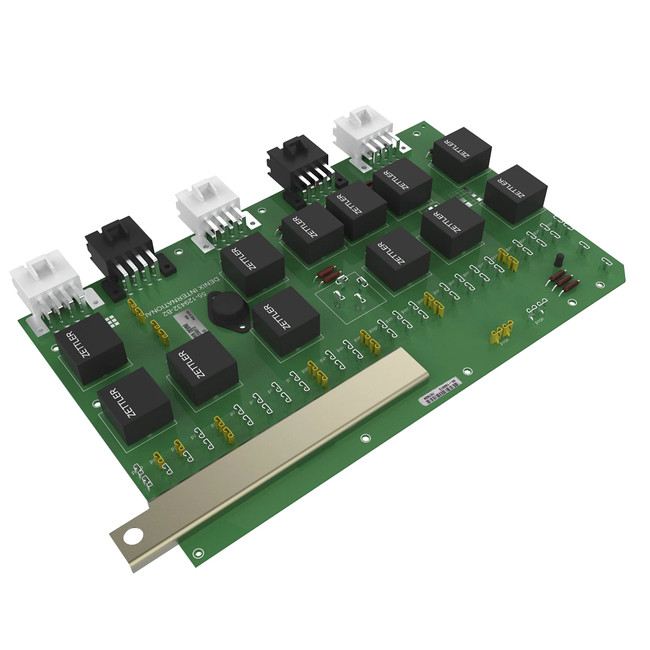
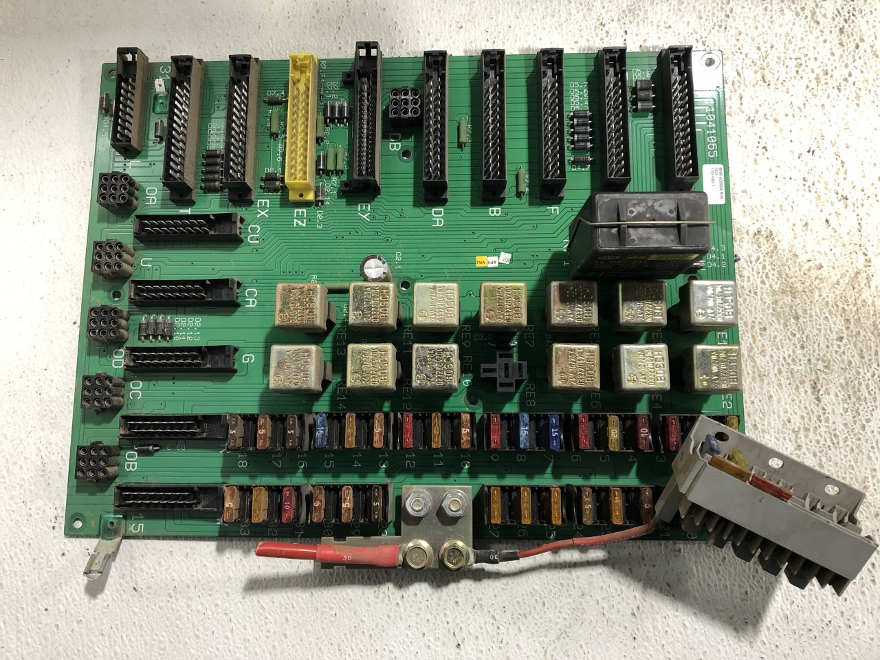
One of the most critical stages in the analysis process involves reconstructing the technical documentation associated with the original PCB. Engineers begin by carefully inspecting each layer to recover copper routing and component placement. During this stage, the schematic diagram, netlist, layout drawing, and Gerber file are gradually recreated through data extraction and electrical verification. The bom list is also reconstructed to identify each component, including microcontrollers, driver ICs, operational amplifiers, and power transistors used to control solenoid valves. Reverse engineering specialists often cross-check the recovered netlist against the recreated schematic diagram to ensure logical accuracy. This phase contains dense technical work where engineers must replicate routing structures, duplicate signal paths, and restore grounding networks before producing a validated Gerber file that can support later reproduction and remanufacture.
La reconstruction de la documentation technique associée à la carte de circuit imprimé de commande hydraulique d’origine est effectuée par les ingénieurs. Ces derniers commencent par examiner minutieusement chaque couche afin de retrouver le routage du cuivre et l’emplacement des composants. Durant cette étape, le schéma, la netlist, le plan d’implantation et le fichier Gerber sont progressivement recréés à partir de la carte de circuit imprimé de commande hydraulique d’origine grâce à l’extraction des données et à la vérification électrique. La nomenclature est également reconstituée pour identifier chaque composant, notamment les microcontrôleurs, les circuits intégrés de commande, les amplificateurs opérationnels et les transistors de puissance utilisés pour commander les électrovannes. Les spécialistes en rétro-ingénierie comparent régulièrement la netlist récupérée avec le schéma de circuit imprimé de commande hydraulique reconstitué afin d’en garantir la cohérence logique. Cette phase implique un travail technique complexe : les ingénieurs doivent reproduire les structures de routage, dupliquer les chemins de signaux et rétablir les réseaux de mise à la terre avant de produire un fichier Gerber validé pour la carte de circuit imprimé de commande hydraulique, permettant ainsi sa reproduction et sa remanufacturation ultérieures.
It has been approved that even if the schematic is correct, the electronic device reliability will be doubted if the PCB card reverse engineering is not well. For example, if the two parallel lines on the PCB card being reverse engineeringed very close to each other, will cause the delay of signal wave transmission, and generate the reflect noise at the end of transmitting line; interference caused by inappropriate consideration of power supply, grounding will degrade the performance of product. As a result of that, when reverse engineering PCB, proper reverse engineering measure must be taken to ensure all the switch power supply can have four current reflow:
Ricostruzione della documentazione tecnica associata alla scheda PCB di controllo idraulico originale. Gli ingegneri iniziano ispezionando attentamente ogni strato per recuperare il routing del rame e il posizionamento dei componenti. Durante questa fase, lo schema elettrico, la netlist, il disegno del layout e il file Gerber vengono gradualmente ricreati dalla scheda PCB di controllo idraulico originale attraverso l’estrazione dei dati e la verifica elettrica. Anche la distinta base viene ricostruita per identificare ciascun componente, inclusi microcontrollori, circuiti integrati di pilotaggio, amplificatori operazionali e transistor di potenza utilizzati per controllare le elettrovalvole. Gli specialisti di reverse engineering spesso confrontano la netlist recuperata con lo schema elettrico della scheda PCB di controllo idraulico ricreato per garantirne l’accuratezza logica. Questa fase prevede un intenso lavoro tecnico in cui gli ingegneri devono replicare le strutture di routing, duplicare i percorsi dei segnali e ripristinare le reti di messa a terra prima di produrre un file Gerber convalidato per la scheda PCB di controllo idraulico che possa supportare la successiva riproduzione e rigenerazione.
1> Power supply switch alternative reflow;
2> Output rectification reflow;
3> Input signal source current reflow;
4> Output overload current reflow;
Input reflow charge the capacitor on the PCB card through direct current resemble when reverse engineering PCB card, wave filtering capacitor play the role of wide band energy storage functions. Similarly, output wave filtering capacitor can be used to store the high frequency energy comes from the rectifier, and eliminate the DC energy of output overload reflow. Consequently, output and input wave filtering capacitor wire connection point is critical when reverse engineering PCB card, if the output/input current reflow and power supply switch fail to connect with connecting point of capacitor, alternative energy can radiate to environment through output or input wave filtering capacitor.
Orijinal Hidrolik Kontrol PCB Kartı ile ilişkili teknik dokümantasyonun yeniden oluşturulması. Mühendisler, bakır yönlendirmesini ve bileşen yerleşimini kurtarmak için her katmanı dikkatlice inceleyerek işe başlarlar. Bu aşamada, şematik diyagram, netlist, yerleşim çizimi ve Gerber dosyası, veri çıkarma ve elektriksel doğrulama yoluyla orijinal Hidrolik Kontrol PCB Kartından kademeli olarak yeniden oluşturulur. Mikrodenetleyiciler, sürücü IC’leri, operasyonel amplifikatörler ve solenoid valfleri kontrol etmek için kullanılan güç transistörleri de dahil olmak üzere her bileşeni tanımlamak için malzeme listesi de yeniden oluşturulur. Tersine mühendislik uzmanları, mantıksal doğruluğu sağlamak için kurtarılan netlisti genellikle yeniden oluşturulan Hidrolik Kontrol PCB Kartı şematik diyagramıyla karşılaştırır. Bu aşama, mühendislerin daha sonraki çoğaltma ve yeniden üretimi destekleyebilecek doğrulanmış bir Hidrolik Kontrol PCB Kartı Gerber dosyası üretmeden önce yönlendirme yapılarını kopyalaması, sinyal yollarını çoğaltması ve topraklama ağlarını geri yüklemesi gereken yoğun teknik çalışma içerir.
Power Supply switch of Alternative route back and rectifier’s AC route back will contain the high level ladder shape current when reverse engineering PCB card, inside this current there are a great deal of harmonic wave which has a much higher frequency then switch basic frequency.
Another important part of PCB card reverse engineering analysis is functional verification and circuit interpretation. Hydraulic control boards typically include feedback circuits that monitor actuator position, current flow, and hydraulic pressure sensors. Engineers must analyze these sections carefully in order to recreate signal filtering, voltage regulation, and protection circuits. During this process, the recreated schematic diagram is compared with actual signal measurements on the board to confirm that the recovered netlist accurately represents real electrical behavior. If obsolete components appear in the bom list, engineers may initiate controlled redesign or redevelopment strategies to maintain functionality while improving component availability. The layout drawing can also be optimized slightly to enhance noise suppression or thermal performance without altering the overall architecture. These adjustments ensure that any replicated or duplicated PCB card maintains compatibility with the backhoe loader’s hydraulic control system.
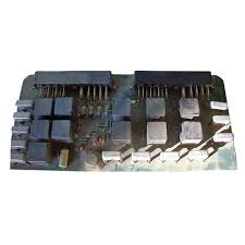
The final stage of reverse engineering analysis focuses on transforming restored documentation into a practical manufacturing solution. Once the schematic diagram, netlist, bom list, layout drawing, and Gerber file have been verified, prototype boards are fabricated to confirm performance. Engineers test the reproduced board with simulated hydraulic loads to ensure that solenoid valve activation and actuator feedback loops respond correctly. Environmental reliability testing may also be performed to evaluate vibration resistance and temperature tolerance in harsh construction environments. After successful validation, the recovered design data becomes a stable foundation for clone production, refurbish programs, or long-term redevelopment of hydraulic control electronics. Through comprehensive PCB card reverse engineering analysis, organizations can confidently reproduce and remanufacture complex control boards while maintaining the reliability required for heavy-duty backhoe loader operations.
ओरिजिनल हाइड्रोलिक कंट्रोल PCB बोर्ड से जुड़े टेक्निकल डॉक्यूमेंटेशन को फिर से बनाना। इंजीनियर कॉपर रूटिंग और कंपोनेंट प्लेसमेंट को रिकवर करने के लिए हर लेयर की ध्यान से जांच करके शुरू करते हैं। इस स्टेज के दौरान, डेटा एक्सट्रैक्शन और इलेक्ट्रिकल वेरिफिकेशन के ज़रिए ओरिजिनल हाइड्रोलिक कंट्रोल PCB बोर्ड से स्कीमैटिक डायग्राम, नेटलिस्ट, लेआउट ड्रॉइंग और गर्बर फ़ाइल को धीरे-धीरे फिर से बनाया जाता है। हर कंपोनेंट की पहचान करने के लिए बॉम लिस्ट को भी फिर से बनाया जाता है, जिसमें माइक्रोकंट्रोलर, ड्राइवर IC, ऑपरेशनल एम्पलीफायर और सोलनॉइड वाल्व को कंट्रोल करने के लिए इस्तेमाल होने वाले पावर ट्रांजिस्टर शामिल हैं। रिवर्स इंजीनियरिंग स्पेशलिस्ट अक्सर लॉजिकल एक्यूरेसी सुनिश्चित करने के लिए रिकवर की गई नेटलिस्ट को फिर से बनाए गए हाइड्रोलिक कंट्रोल PCB बोर्ड स्कीमैटिक डायग्राम से क्रॉस-चेक करते हैं। इस फेज़ में बहुत ज़्यादा टेक्निकल काम होता है जहाँ इंजीनियरों को रूटिंग स्ट्रक्चर को कॉपी करना होता है, सिग्नल पाथ को डुप्लिकेट करना होता है, और एक वैलिडेटेड हाइड्रोलिक कंट्रोल PCB बोर्ड की गर्बर फ़ाइल बनाने से पहले ग्राउंडिंग नेटवर्क को रिस्टोर करना होता है जो बाद में रिप्रोडक्शन और रीमैन्युफैक्चरिंग में मदद कर सके।