


PCB Reverse Engineering: BGA Net Extraction Without Reflow
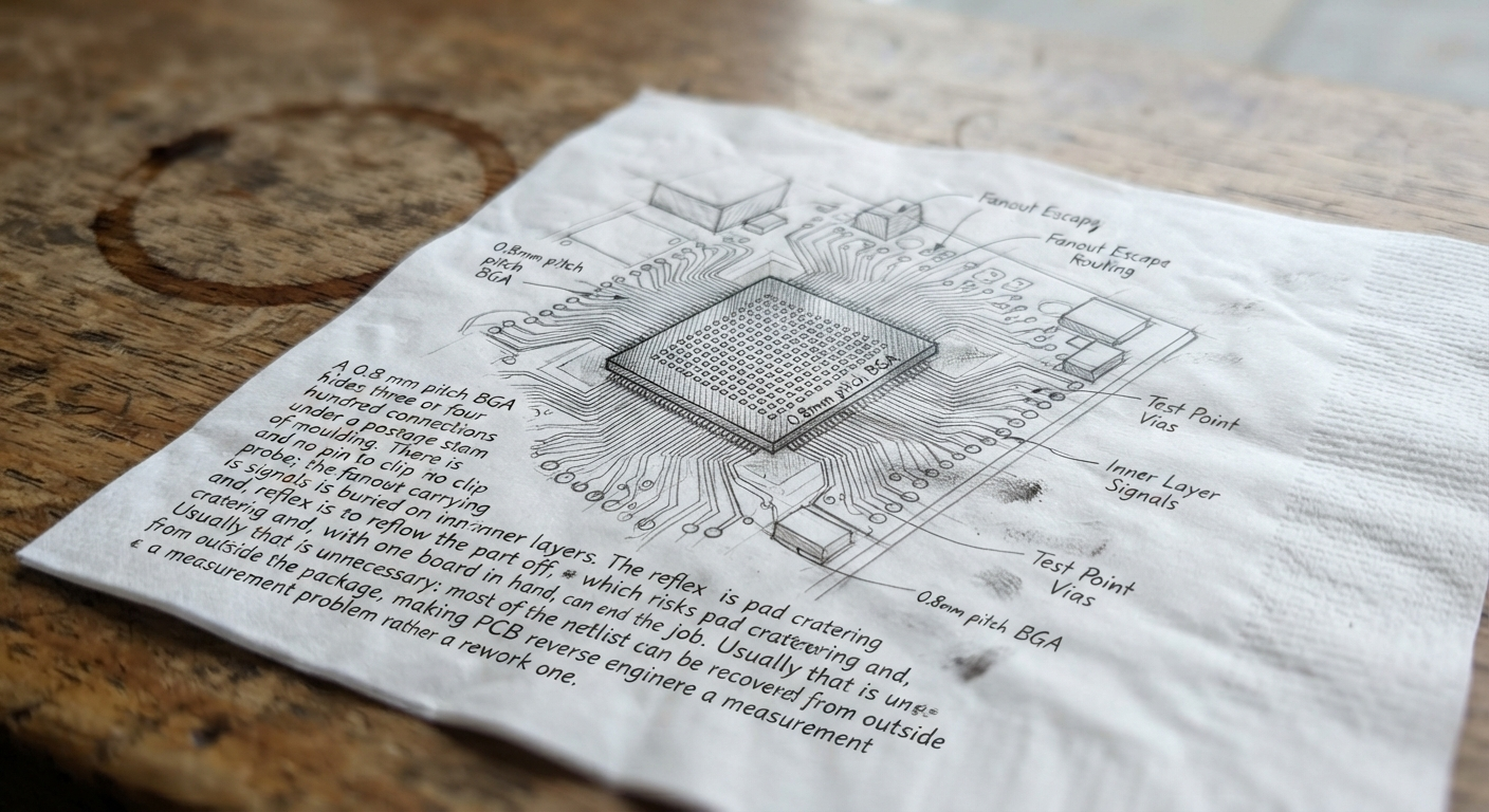
A 0.8 mm pitch BGA hides three or four hundred connections under a postage stamp of moulding. There is no lead to clip and no pin to probe; the fanout carrying those signals is buried on inner layers. The reflex is to reflow the part off, which risks pad cratering and, with one board in hand, can end the job. Usually that is unnecessary: most of the netlist can be recovered from outside the package, making PCB reverse engineering here a measurement problem rather than a rework one.
Why ball-grid packages break the usual method
The standard method assumes two endpoints: follow a trace to a component, touch the lead, confirm continuity. A ball-grid array removes both at once. The connection is a 0.3 mm sphere under the body, and the trace leaving it dives into a via within a millimetre. At 0.4 mm pitch the escape channels are 0.1 mm wide, laser-drilled microvias often filled and capped, so even the via mouth sits under mask.
What remains is indirect: imaging through the package, the device’s own test logic, and inference from the few reachable nodes.
Reading the ball field
Start with 2D X-ray transmission. A microfocus source at high magnification shows the ball array, missing or bridged balls, voiding and, most usefully, the shadow of each fanout via just outside its pad. Ball and via diameters tell them apart. At 0.5 mm pitch the limit is spot size, not detector resolution.
Computed laminography
Rotating source and detector and reconstructing slices resolves depth — useful when a trace dives from a ball to an inner layer. Planar samples restrict the angular range, so expect streaks; use it to answer one question — whether one ball reaches one via — not to image a whole board. Copper at 35 micrometres in a 1.6 mm stack gives weak contrast: you read via barrels and plane edges, not traces.
The deliverable of this PCB reverse engineering step is a ball-to-via map; cross it with the datasheet ball map and every net gains a signal name before a probe touches the board.
Letting the device test itself
If the BGA is a processor, FPGA or CPLD it probably has a JTAG port. IEEE 1149.1 boundary scan drives and samples pins from inside the package, and an interconnect test between two boundary-scan devices recovers every net joining them — no probing, and the output is already a netlist. Two limits: nets to parts without boundary scan stay unresolved, and you need BSDL files plus a working chain. If the chain is broken, repair it first — one missing TDO link invalidates the run.
Probing what JTAG cannot reach
For the remainder, a flying probe with 0.1 mm tips reaches via annuli, test pads and pins. Tented vias need the mask opened locally — fine on a coupon, risky on a signal you cannot replace. Measure differential pairs as pairs: a 100 Ω termination reads as a short to a continuity tester. Capacitance signature and time-domain reflectometry help where a net vanishes into a plane; a second board turns ambiguity into comparison.
When the package has to come off
Some nets never surface: power and ground balls dropping straight into a plane, analog nodes routed beneath the body. Removal is then justified — a planned step, not a reflex.
Bake first, per J-STD-033: trapped moisture turns a reflow into delamination. Preheat the underside to 125–150 °C, apply low-melt alloy to lower working temperature, then lift with hot air and vacuum. What you gain: every ball pad becomes a probe point and the escape routing shows. What you lose: the assembly, possibly the board if a pad craters.
The order that works
Non-destructive evidence first, always — it cannot be re-collected, and in PCB reverse engineering the sequence is the method:
- Photograph both sides and all four package edges at magnification.
- X-ray the ball field; build the ball-to-via map and label it from the datasheet.
- Run boundary scan where a chain exists; export the interconnect results.
- Flying-probe the accessible nodes; resolve differential pairs and plane ties.
- Lift the package only after steps one to four are archived.
- Reconcile every source into one netlist and log conflicts as open questions.
Circuit Engineering Company Limited works on industrial boards — PLC racks, drive stages, switch-mode supplies — starting from the physical board and delivering editable data the client owns. On ball-grid assemblies the netlist goes into schematic recovery carrying a confidence note per node, so whoever draws the schematic knows which connections were measured and which inferred, while the reverse engineering workflow keeps X-ray and boundary-scan evidence with the revision it belongs to.
A BGA is not a wall. It hides its connections and rewards a sequence: image first, test from inside second, probe what is left third, only then consider heat. Boards that survive that order come back with a defensible netlist.