


HMI Board Reverse Engineering: Display Drivers and Keypads
A machine operator panel is the most handled board in the plant and the least documented. Membrane overlays wear through, LCDs fade at the edges, and the controller that drove them was discontinued a decade ago. Yet the panel is often the only interface the process has, so it has to be understood before it can be repaired or rebuilt. The complication is that an HMI concentrates several interfaces on one small board: a display bus, a keypad scan matrix, a backlight supply and a link to the PLC. PCB reverse engineering of an operator panel is therefore several recovery problems at once, each with its own timing rules.
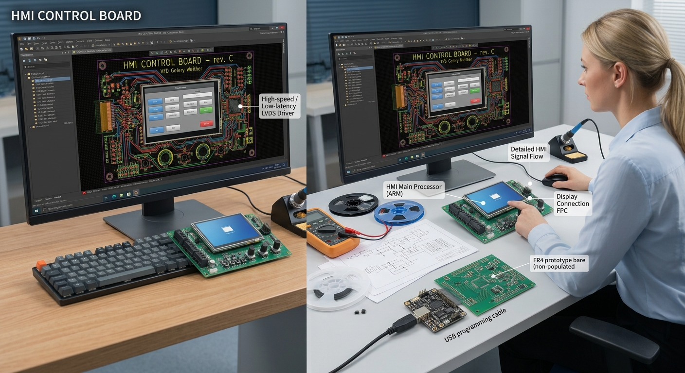
What an operator panel actually contains
Start with the physical stack: overlay, keypad, display module, main board, and behind them a backlight board or a communication board. The main board carries the processor or dedicated HMI controller, the display connector, the keypad connector, the backlight driver, the serial transceiver to the PLC and the configuration memory. Three attributes decide how hard the recovery will be:
- Interface type — a 16-bit parallel 8080 bus, a serial SPI link, or an LVDS differential pair.
- Display driver — whether the module owns a register set you can read, or is raw glass driven by the host.
- Configuration storage — whether screen data and keypad mapping live in firmware, an EEPROM or battery-backed RAM.
The last of the three usually disappears first, and its loss is what forces the work.
Recovering the display interface
Parallel buses
Legacy panels most often use an 8080-style bus: eight or sixteen data lines, write, read, chip select, register select and reset. Trace them as a group and verify each by continuity, because a single misidentified line changes nothing on a multimeter and everything on a screen. Register select deserves special care: it separates command writes from data writes inside the display controller, and it is easily swapped with chip select during a repair.
Serial and SPI displays
Later modules use SPI with a data/command pin, or I²C for small character displays. A first HMI board reverse engineering pass should establish the clock rate and the command set before anything else. Cheaper modules accept commands only, so no status is readable over the bus and behaviour must be inferred from what appears on the glass. Verify timing against the controller datasheet, and expect connector pinout to differ from the module’s internal order.
Backlight and bias rails
A backlight is a power design in miniature: a constant-current boost converter for LEDs, a high-voltage inverter for older CCFL tubes, a negative bias rail for LCD contrast. This is where obsolete electronic components concentrate, and where substitutes must match current regulation rather than pinout. Measure the rails under load and record the dimming method — PWM on an enable pin, an analog reference, or a current-sense divider.
The keypad matrix and how it is scanned
A matrix keypad is read by driving rows and sensing columns, with firmware deciding the scan order. Ghosting diodes, if present, tell you the panel tolerates multi-key presses; their absence forbids certain combinations. The membrane keypad ribbon is the most common field failure, and its connector often shares a common return with the display, so isolation must be verified before assuming a controller fault. Recover the mapping by measuring while keys are pressed, then record it as a table alongside the netlist.
A recovery sequence for HMI boards
Order matters here as much as anywhere:
- Photograph the assembled panel, the overlay and both board sides before disassembly.
- Extract the netlist, giving the display and keypad connectors the highest priority.
- Identify the display controller, the keypad scan port and the communication transceiver.
- Rebuild the schematic by continuity, marking measured values apart from inferred ones.
- Power the panel safely and capture bus traffic while the screen updates and keys are pressed.
- Verify the rebuilt mapping against the original before releasing any data.
Step five is where most PCB reverse engineering of a panel is won or lost, because a captured frame says more about the register map than any amount of tracing.
How this work is approached
Our team at Circuit Engineering Company Limited focuses on industrial boards of this kind, including operator panels, recovered from the physical board and delivered as editable data the client owns — netlist, schematic, fabrication data and a bill of materials. A panel recovered this way stays maintainable through a documented schematic recovery route instead of being scrapped, which is the same reasoning behind PCB cloning engagements and the wider industrial board family.
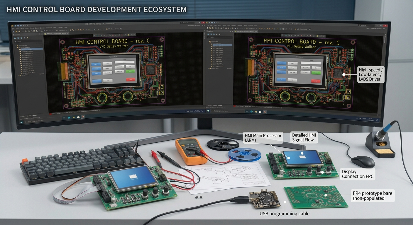
Panels fail slowly and then completely. Read the interfaces in order — bus, display, backlight, keypad — and PCB reverse engineering turns a dead operator station back into a documented design.