

How to guarding PCB static effect basic principle
Guarding basic principles are simple: Completely surround sensitive nodes with conductors that can readily sink stray currents, and maintain the guard conductors at the exact potential of the sensitive node (as otherwise the guard will serve as a leakage source rather than a leakage sink). For example, to keep leakage into a node below 1 pA (assuming 1000-megohm leakage resistance) the guard and guarded node must be within 1 mV. Generally, the low offset of a modern op amp is sufficient to meet this criterion.
There are important caveats to be noted with implementing a true high quality guard. For traditional through hole PCB connections, the guard pattern should appear on both sides of the circuit board, to be most effective. And, it should also be connected along its length by several vias. Finally, when either justified or required by the system design parameters, do make an effort to include guards in the PCB design process from the outset—there is little likelihood that a proper guard can be added as an afterthought.
Figure below illustrates the case for a noninverting guard. In this instance the op amp reference input is directly driven by the source, which complicates matters considerably. Again, the guard ring completely surrounds all of the input nodal connections. In this instance, however, the guard is driven from the low impedance feedback divider
connected to the inverting input.
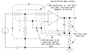
Noninverting Mode Guard Encloses all Op Amp Noninverting Input
Usually the guard-to-divider junction will be a direct connection, but in some cases a unity gain buffer might be used at “X” to drive a cable shield, or also to maintain the lowest possible impedance at the guard ring. In lieu of the buffer, another useful step is to use an additional, directly grounded screen ring, “Y,” which surrounds the inner guard and the feedback nodes as shown. This step costs nothing except some added layout time, and will greatly help buffer leakage effects into the higher impedance inner guard ring.
Of course what hasn’t been addressed to this point is just how the op amp itself gets connected into these guarded islands without compromising performance. The traditional method using a TO-99 metal can package device was to employ double-sided PCB guard rings, with both op amp inputs terminated within the guarded ring.