PCB Reverse Engineering, PCB Clone & PCB Copy Services

PCB Reverse Engineering Sketches

In the intricate world of electronics, where technology evolves rapidly, many legacy systems become obsolete—not because they stop working, but because their supporting documentation disappears. For companies or individuals working with phased-out circuit boards, one of the most powerful tools available today is the creation of PCB reverse engineering sketches.
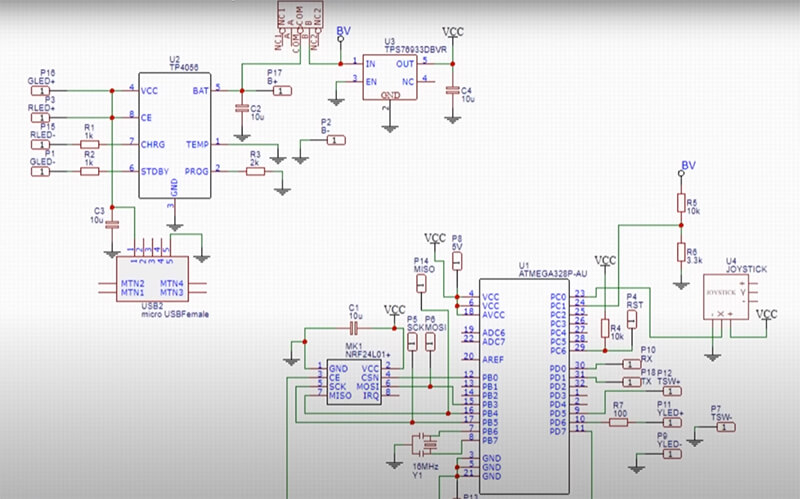
Szkice inżynierii odwrotnej PCB to wstępne graficzne reprezentacje fizycznej PCB, tworzone po szczegółowej inspekcji i pomiarach. Szkice te mapują rozmieszczenie komponentów, trasowanie ścieżek, przepływ sygnału i struktury warstw. Działają jako punkt wyjścia do tworzenia precyzyjnych wyników cyfrowych, takich jak:
Pliki Gerber do produkcji PCB
Schematy schematyczne do zrozumienia obwodów
Rysunki układów do powielania projektu
Listy BOM (zestawienie materiałów) do pozyskiwania komponentów
Listy połączeń do weryfikacji łączności elektrycznej
W przeciwieństwie do standardowych plików CAD generowanych z oryginalnych projektów, szkice inżynierii odwrotnej są ręcznie konstruowane w oparciu o analizę w świecie rzeczywistym. Ten proces łączy lukę między sprzętem fizycznym a danymi cyfrowymi, zwłaszcza gdy oryginalne pliki PCB są nieobecne lub nigdy nie istniały.
Szkice inżynierii odwrotnej PCB to wstępne graficzne reprezentacje fizycznej PCB, tworzone po szczegółowej inspekcji i pomiarach. Szkice te mapują rozmieszczenie komponentów, trasowanie ścieżek, przepływ sygnału i struktury warstw. Działają jako punkt wyjścia do tworzenia precyzyjnych wyników cyfrowych, takich jak: Pliki Gerber do produkcji PCB Schematy schematyczne do zrozumienia obwodów Rysunki układów do powielania projektu Listy BOM (zestawienie materiałów) do pozyskiwania komponentów Listy połączeń do weryfikacji łączności elektrycznej W przeciwieństwie do standardowych plików CAD generowanych z oryginalnych projektów, szkice inżynierii odwrotnej są ręcznie konstruowane w oparciu o analizę w świecie rzeczywistym. Ten proces łączy lukę między sprzętem fizycznym a danymi cyfrowymi, zwłaszcza gdy oryginalne pliki PCB są nieobecne lub nigdy nie istniały.

These technical sketches serve as the foundation for reconstructing a complete, accurate digital model of the original PCB, allowing engineers to recover, restore, or recreate missing documentation and hardware for long-discontinued devices.

PCB reverse engineering sketches are preliminary graphical representations of a physical PCB, created after detailed inspection and measurement. These sketches map out component placements, trace routing, signal flow, and layer structures. They act as the starting point for producing precise digital outputs, such as:

  • Gerber files for PCB fabrication
  • Schematic diagrams for circuit understanding
  • Layout drawings for design replication
  • BOM lists (Bill of Materials) for sourcing components
  • Netlists for verifying electrical connectivity

Unlike standard CAD files generated from original designs, reverse engineering sketches are manually constructed based on real-world analysis. This process bridges the gap between physical hardware and digital data, especially when the original PCB files are missing or never existed.
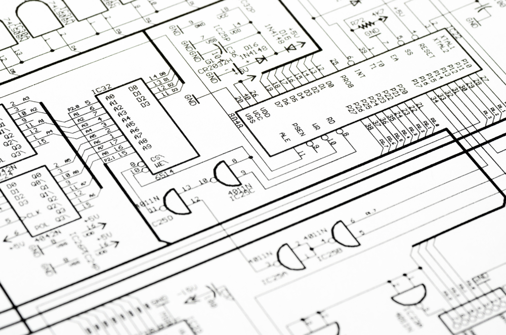
PCB 역설계 스케치는 실제 PCB의 세부 검사 및 측정 후 생성된 예비 그래픽 표현입니다. 이 스케치는 부품 배치, 트레이스 라우팅, 신호 흐름 및 레이어 구조를 매핑합니다. 다음과 같은 정밀한 디지털 출력물을 생성하는 시작점 역할을 합니다.
PCB 제조를 위한 거버 파일
회로 이해를 위한 회로도
설계 복제를 위한 레이아웃 도면
부품 조달을 위한 BOM 목록(자재 명세서)
전기적 연결 검증을 위한 넷리스트
원래 설계에서 생성된 표준 CAD 파일과 달리, 역설계 스케치는 실제 분석을 기반으로 수작업으로 작성됩니다. 이 프로세스는 특히 원본 PCB 파일이 없거나 존재하지 않았을 때 물리적 하드웨어와 디지털 데이터 간의 차이를 메우는 데 효과적입니다.
PCB 역설계 스케치는 실제 PCB의 세부 검사 및 측정 후 생성된 예비 그래픽 표현입니다. 이 스케치는 부품 배치, 트레이스 라우팅, 신호 흐름 및 레이어 구조를 매핑합니다. 다음과 같은 정밀한 디지털 출력물을 생성하는 시작점 역할을 합니다. PCB 제조를 위한 거버 파일 회로 이해를 위한 회로도 설계 복제를 위한 레이아웃 도면 부품 조달을 위한 BOM 목록(자재 명세서) 전기적 연결 검증을 위한 넷리스트 원래 설계에서 생성된 표준 CAD 파일과 달리, 역설계 스케치는 실제 분석을 기반으로 수작업으로 작성됩니다. 이 프로세스는 특히 원본 PCB 파일이 없거나 존재하지 않았을 때 물리적 하드웨어와 디지털 데이터 간의 차이를 메우는 데 효과적입니다.

For businesses dependent on legacy systems, especially in industrial, medical, military, or telecom sectors, phase-out circuit boards often represent a serious risk. A single faulty or unsupported board can halt operations. In many cases, the OEM no longer exists or no longer supports the product. That’s where sketches created during PCB reverse engineering come in.

By developing and refining these hand-drawn or digitally-assisted sketches, engineers can replicate, clone, or remanufacture boards with high accuracy. These sketches also serve as a vital reference during redevelopment or redesign, offering insight into the original engineering intent, allowing for component substitutions, layout improvements, or updated compliance modifications.

The value of PCB reverse engineering sketches goes beyond just rebuilding a board. For companies, these sketches become part of a restored technical archive, useful for future repairs, in-house production, or migration to newer platforms. For individuals or small developers, the sketches offer an affordable entry point into reproducing old boards, avoiding full redesign from scratch.

Additionally, sketches can be annotated with performance observations, thermal zones, or EMI-sensitive areas, aiding in further refurbishment, testing, or optimization of the circuit.

Before a reverse-engineered Gerber file can be generated or a BOM list completed, the project must start somewhere—and that place is often the PCB reverse engineering sketch. It is the roadmap that makes it possible to duplicate what once seemed unrecoverable.
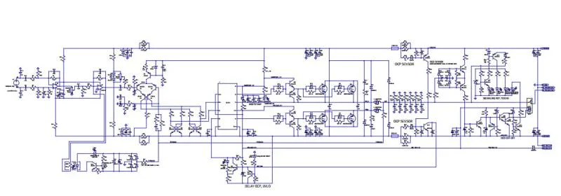
Gli sketch di reverse engineering per PCB sono rappresentazioni grafiche preliminari di un PCB fisico, create dopo un'ispezione e una misurazione dettagliate. Questi sketch mappano il posizionamento dei componenti, il routing delle tracce, il flusso del segnale e la struttura dei livelli. Costituiscono il punto di partenza per la produzione di output digitali precisi, come:
File Gerber per la fabbricazione del PCB
Diagrammi schematici per la comprensione del circuito
Disegni di layout per la replica del progetto
Liste BOM (Bill of Materials) per l'approvvigionamento dei componenti
Netlist per la verifica della connettività elettrica
A differenza dei file CAD standard generati dai progetti originali, gli sketch di reverse engineering vengono creati manualmente sulla base di analisi reali. Questo processo colma il divario tra hardware fisico e dati digitali, soprattutto quando i file PCB originali sono mancanti o non sono mai esistiti.
Gli sketch di reverse engineering per PCB sono rappresentazioni grafiche preliminari di un PCB fisico, create dopo un’ispezione e una misurazione dettagliate. Questi sketch mappano il posizionamento dei componenti, il routing delle tracce, il flusso del segnale e la struttura dei livelli. Costituiscono il punto di partenza per la produzione di output digitali precisi, come: File Gerber per la fabbricazione del PCB Diagrammi schematici per la comprensione del circuito Disegni di layout per la replica del progetto Liste BOM (Bill of Materials) per l’approvvigionamento dei componenti Netlist per la verifica della connettività elettrica A differenza dei file CAD standard generati dai progetti originali, gli sketch di reverse engineering vengono creati manualmente sulla base di analisi reali. Questo processo colma il divario tra hardware fisico e dati digitali, soprattutto quando i file PCB originali sono mancanti o non sono mai esistiti.

In an age where electronic obsolescence is a costly reality, PCB reverse engineering sketches offer a powerful solution. Whether the goal is to recreate documentation, restore functionality, or redevelop hardware for new use cases, these sketches are the foundation for turning legacy boards into viable, modern-ready assets.