

ESD effect when Clone PWB Board
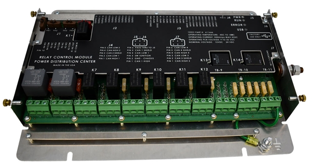
In the process of cloning PWB board of Power Distribution & Relay Control devices, Electrostatic Discharge (ESD) is an often-underestimated factor that can significantly affect the accuracy and reliability of reverse engineering results. These circuit boards are widely used in excavator auxiliary systems, including lighting control, relay switching, and power routing for secondary functions. During reverse engineering, improper ESD control may lead to latent damage, functional deviation, or data inconsistency when attempting to recover, copy, or replicate the original design.
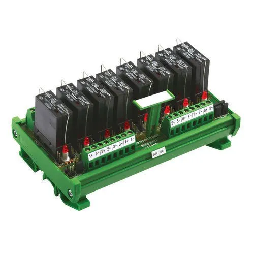
Power distribution and relay control PWB boards typically integrate discrete power components, relay drivers, MOSFETs, protection diodes, and microcontroller or logic interfaces. When engineers extract a schematic diagram, generate a netlist, or recreate a layout drawing, ESD events can alter component parameters or partially degrade semiconductor junctions. These failures are not always immediately detectable but can cause malfunction after reproduce or remanufacture of the PCB.
The action need to prevent the negative effect of ESD on them, in order to minimize the negative effect and have a better PWB Board clone outcome, below measures must be made to ensure the goal being achieved:
1. cabinet grounding track on the top and bottom shouldn’t print mask resist then it can be the discharge electrode for pwb board clone if the board is put outside of metal cabinet or shielding box;
2. Design a round grounding on the circuit:
1> Loop circuit being placed when clone pwb board except the rim connector and cabinet grounding;
2> ensure all the annular ring width greater than 2.5mm;
3> connect the annular ring by through vias each 13mm;
4> connect the common grounding of multilayer circuit with annular ring grounding;
5> as for the double side pwb board installed outside metal cabinet or shielding, should put the annular ring grounding with common circuit;
3. clone pwb board a grounding track aside each one of signal track in where the ESD can be penetrated directly;
4. I/O circuit should be cloneed to close the corresponding connector;
5. for those circuits which are more susceptible to ESD, should be clone in the centre area of pwb board, because other circuits can provide the protection for them;
6. clone series resistor and magnetic bead on the receiving terminal, as for those cable driver which is more liable to get shock by ESD, can also consider clone pwb board with resistor and magnetic bead at the receiving terminal;
7. instant protector normally should be placed on the receiving terminal of pwb board. Use the short and thick wire connect the cabinet grounding.
During the clone and duplicate stages, the original board must be carefully handled while stripping solder mask, exposing copper tracks, and desoldering components for BOM list verification. At this stage, ESD may be introduced through manual probing, imaging equipment, or insufficient grounding. Sensitive relay control ICs, signal conditioning circuits, and GPIO interfaces used for excavator lighting control are particularly vulnerable. If ESD damage occurs, the restored Gerber file or schematic diagram may reflect incorrect signal paths or unstable logic behavior, leading to faulty redeployment.
A professional reverse engineering workflow must therefore integrate ESD mitigation as part of the documentation recovery process. This includes antistatic workstations, grounded tools, controlled humidity, and ESD-safe desoldering procedures. By doing so, engineers can accurately restore, recreate, and redesign the original PWB without introducing artificial defects that compromise system performance.
Once ESD-safe data acquisition is complete, the collected information—including schematic diagram, layout drawing, netlist, and BOM list—can be confidently used for refurbish, redevelopment, or full production replication. This is particularly important when converting reverse-engineered documents into functional prototypes for excavator auxiliary power distribution and relay-based lighting control systems.
In conclusion, understanding the existence and impact of ESD during cloning PWB board processes is essential for ensuring technical integrity. Proper ESD control not only protects the physical PCB but also guarantees that the digital assets generated through copy, replicate, and reverse engineering accurately represent the original design, enabling reliable manufacturing, maintenance, and long-term system support.
Nowadays, electronic products are being updated in fast speed; and PWB board CLONE from our company in the base of completely master the traditional PWB board structure or its basic circuit, furthermore, is base upon the self research and development, include the software upgrade and product second phase development; and we will dedicate to clone PCB with 100% exact the same functions as original sample given by customers.at the same time, we also decrease the PWB BOARD clone cycle refers to the pcb board with blind or buried vias, effectively save customer time and energy, low down its cost. and which is also one of the reasons for us to be favor by most of our clients.