

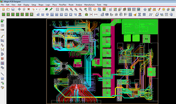
Clone PCB Circuit Board Layout Schematic
Clone PCB Circuit Board Layout Schematic needs to consider the routing channel and via area. These paths and areas are obvious to the designer, but the automatic routing tool only considers one signal at a time. By setting routing constraints and setting the layers of the signal line, the routing tool can be as the designer imagined to complete the wiring design like that.
In the fan-out design stage, to enable automatic routing tools to connect component pins, each pin of the surface mount device should have at least one via, so that when more connections are needed, the circuit board can be internally layered Connection, online testing (ICT) and circuit reprocessing.
In order to maximize the efficiency of the automatic routing tool for reverse engineering printed wiring board, the largest via size and printed line must be used as much as possible, and the interval is set to 50mil. Use the via type that maximizes the number of routing paths.
When carrying out fan-out design, it is necessary to consider the circuit online test. Test fixtures can be expensive and are usually ordered when pcb board about to be put into full production after reverse engineering printed circuit board. If only then consider adding nodes to achieve 100% testability, it would be too late.