

Double Layer Printed Circuit Board Reverse Routing
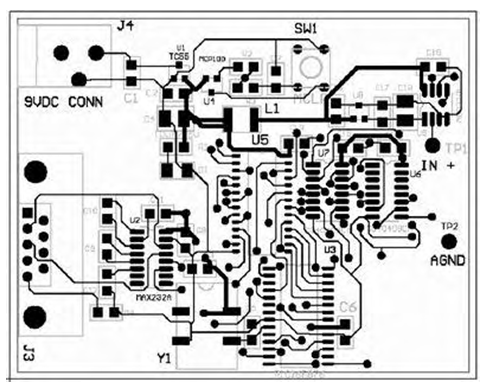
Below Figure shows the top layer of a Double Layer Printed Circuit Board Reverse Routing layout design.
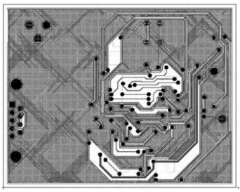
The bottom layer of Double side PCB board Reverse engineering is shown in below Figure, and the circuit schematics of these wiring layers are shown in Figure 3a and Figure 3b.
When reverse engineering this mixed-signal circuit board, after careful consideration, the devices were manually placed on the board to separate the digital and analog devices.
When adopting this kind of wiring scheme, there are several aspects that need attention, but the most troublesome is grounding. If the ground wire is routed on the top layer, the devices on the top layer are all grounded through traces.
The device is also grounded on the bottom layer, and the ground wires on the top and bottom layers are connected through the vias on the far right side of the circuit board.
When checking this kind of wiring strategy, the first drawback is that there are multiple ground loops. In addition, you will find that the ground return path of the bottom layer is interrupted by the horizontal signal line.
The desirability of this grounding scheme is that the analog components (12-bit A/D converter MCP3202 and 2.5V reference voltage source MCP4125) are placed on the far right side of the circuit board. This layout ensures that there will be no under these analog chips.