

Voltage Drop in PCB Signal
The gain error resulting from resistive voltage drop in PCB signal leads is important only with high precision and/or at high resolutions, or where large signal currents flow. Where load impedance is constant and resistive, adjusting overall system gain can compensate for the error. In other circumstances, it may often be removed by the use of “Kelvin” or “voltage sensing” feedback.
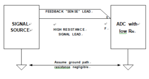
In this modification to the case of Figure above, a long resistive PCB trace is still used to drive the input of a high resolution ADC, with low input impedance. In this case however, the voltage drop in the signal lead does not give rise to an error, as feedback is taken directly from the input pin of the ADC, and returned to the driving source. This scheme allows full accuracy to be achieved in the signal presented to the ADC, despite any voltage drop across the signal trace.
Use of a Sense Connection Moves Accuracy to the Load Point
The use of separate force (F) and sense (S) connections (often referred to as a Kelvin connection) at the load removes any errors resulting from voltage drops in the force lead, but, of course, may only be used in systems where there is negative feedback. It is also impossible to use such an arrangement to drive two or more loads with equal accuracy, since feedback may only be taken from one point. Also, in this much-simplified system, errors in the common lead source/load path are ignored, the assumption being that ground path voltages are negligible. In many systems this may not necessarily be the case, and additional steps may be needed, as noted below.