

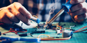
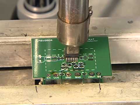
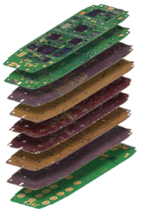
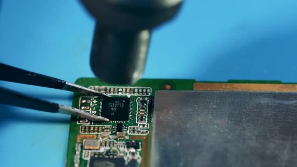
PCB Board Reverse Engineering Inspection
PCB Board Reverse Engineering need to check the circuit pattern quality, electrical connection and track route stability and rationality. The items for pcb board reverse engineering checking include:
1 tracks can be short and straight without the sacrifice of functions;
2 if the reverse engineering has followed the limitation rules for track width;
3 among the tracks, tracks and fixed holes, tracks and soldering pads, if sufficient space has been saved for them;
4 if all the tracks have already avoided the parallel tracks (include the component leads);
5 if the sharp angle has been avoid;
6 check if the PCB schematic diagram is rational and correct;
7 check if all the component packages are all correct and rational;
8 strong and weak electricity distance and the space between blocked areas;
9 check the schematic and PCB drawing correspondingly to avoid the lost of netlist;
10 if the footprint of component can match with physical sample;
11 if the placement of components are all properly;
—1 if the components are all easy to assemble and dissemble;
—2 if the thermal sensitivity components are far away enough with thermal dissipation parts;
—3 those components can cause intercourse affection has proper orientation and locations;
—4 the locations of each one of insert and dip parts are all placed properly;
12. components with orientation are rotation wrongly instead of switching;
13. pin lead of components with dual insert package are properly reverse engineering and easy to insert;
14. check if any one of the component are normal and without any leak;
15. check if there is through vias on the upper and down layer, and the soldering pads are connected by through vias to prevent the tracks break off, ensure the completeness of circuit tracks;
16. check if the silkscreen marking on the up and down layers are properly placed, don’t put the components on the markings for the sake of soldering and maintenaince operation;
Tags: pcb assemble reverse engineering,pcb board reverse engineering,pcb card reverse engineering,pcb reverse engineering,pcba reverse engineering,Printed Circuit Board Reverse Engineering,printed wiring board reverse engineering,pwb reverse engineering,pwba reverse engineering