

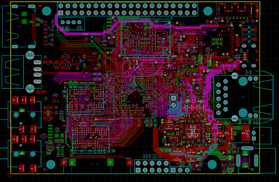
Reverse Engineering Printed Wiring Board Layout Signal Track on the ground layer
When reverse engineering Printed Wiring Board, due to the quantity of residue tracks on the signal layer won’t left too much, and add an extra layer onto the whole PCB Board velocity measurement Reverse Engineering will increase much more workload and production cost, in order to solve this conflict, engineer will consider layout the tracks on the ground layer. First of all, it will consider use the power supply layer, then it is the ground layer. Because the best option is save the integrity of ground layer.
Connecting Pin in the large area of conductor in Printed circuit board Reverse Engineering
When reverse engineering PCB display adjustment, one of the commonly issue is the way of components pin or lead connecting on the large area ground layer, and the operation on the connecting pin must take comprehesive consideration, as for the electrical features, the soldering pad for the components lead should layout completely with copper area when PCB reverse engineering, but there are also several drawbacks of this kind of method, for example:
1, heater with higher power must be used to fulfill the soldering in the forthcoming Printed Wiring Board assemble;
2, cold soldering point could more possible be generated;
So in order to take both the electrical/eletronic features and manufacturing characteristic into account, cross soldering pad can be designed, which also known as heat shield , or thermal shield.
In that scenario, the possiblity of cold soldering point in the process of Printed Wiring Board assemble due to the over-thermal dissipation will be decreased dramatically. This method can also be applied onto the multilayer PCB reverse engineering project.
Tags: pcb board reverse engineering,pcb card reverse engineering,pcb reverse engineering,pcba reverse engineering,Printed Circuit Board Reverse Engineering,printed wiring board reverse engineering,pwb reverse engineering,pwba reverse engineering