

Reverse Engineering Printed Circuit Board Schematic
We are now ready to actually reverse engineering printed circuit board schematic from the physical sample. There is no information about physical data in a schematic – orientation, spacing, and the like mean nothing. The only data that will be sent to the printed circuit board document besides a list of what nodes are connected to each other (a netlist) are the number of pins on each part, and the Footprint for each part. The latter is where physical data comes into play.
A Footprint is a graphical symbol that shows where each pin of a device is physically located. We still must enter this information before we can create the printed circuit board. The printed circuit board Libraries are in C:\Program Files\Design Explorer 99SE\Library\printed circuit board.
While Reverse Engineering Printed Circuit Board Schematic elsewhere, create circuit boards that are covered with a laminating material, the T-Tech Machine at MIL creates circuit boards that are just exposed layers of copper. Therefore, soldering to these boards can be more difficult then soldering to a regular printed circuit board. We therefore use special printed circuit board libraries for T-Tech Boards – they are located in C:\Program Files\Design Explorer 99SE\Library\printed circuit board\Generic Footprints\MLL_printed circuit board.DDB.
Open up MIL_printed circuit board.DDB – you’ll see several .LIB files in the Documents folder. These are printed circuit board Footprint Libraries. If you open up SHEET1.LIB and SHEET1OB.LIB, you will notice they have the same footprints, with the only difference being that the latter has oval, or oblong, pads (the dark gray) instead of circles like SHEET1. The Oblong pads are easier to solder to, and should always be used when possible if you are making a copper clad board.
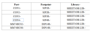
We use the following footprints for each part:
footprints for each part