

PCB Circuit Board Reverse Engineering Design Rules Checking
Design Rule checking is critical for the PCB circuit board Reverse Engineering process, after the PCB circuit board layout has been done, engineer should check if the layout design is completely align with the design rule sets by the designer, at the same time, they need to confirm if these setting rules can satisfy the requirement of PCB circuit board manufacturer after reverse engineering process done. And there are below rules need to follow up:
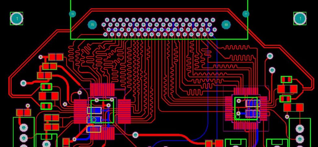
1, the distance between the tracks, tracks and soldering pad, track and through hole, soldering pad and through hole, through holes can meet the minimum requirement of PCB circuit board manufacture;
2, the space between the power supply track and ground tracks after reverse engineering pcb display adjustment is appropriate or not, the distance between power supply track and ground track is closely decoupling with low wave resistance value. And if there is any place on the PCB circuit board pattern to widen the space;
3, is there any optimum measure can be taken for the critical signal track such as the shortest length, add protective track and separate the input and output line distinctively;
4, if there is any isolated ground line in the digital circuit and analog circuit after PCB reverse engineering by orcad software;
5, is there any technical track on the PCB circuit board layout, and solder resist can meet the manufacturing requirement, the size and dimensio and solder resist is properly layout? All of the legendary marking has been printed properly without any encroaching on the soldering pad?
The external outline frame on the power supply ground layer has been shrinked after PCB reverse engineering to avoid the copper exposure in the process of PCB circuit board manufacturing;
Tags: pcb board reverse engineering,pcb card reverse engineering,pcb circuit board reverse engineering,pcb reverse engineering,pcba reverse engineering,Printed Circuit Board Reverse Engineering,printed wiring board reverse engineering,pwb reverse engineering,pwba reverse engineering