

Reverse Engineering PCB India
Reverse Engineering PCB India
As we know that Reverse Engineering PCB India final purpose is to produce an workable functional prototype which possess the same or more advanced technology. Then Post-shipment inspection can preclude the replication of defects, the hardware provided for pcb reverse engineering should be inspected for possible damage in shipment.
The necessary documentation for control such as Damage Reports or Failed Item Reports, should be generated as required. An initial operating test should be performed to ensure the item functions in accordance with established performance specifications.
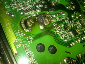
Pre-disassembly photographs, The hardware should be photographed prior to and during disassembly since, in some cases, no other record of the item exists. In addition, since the piece-parts will be identified by bagging and tagging, their position in the assembly should be noted.
Tags: PCB Reverse Engineering china,PCB Reverse Engineering india,PCB Reverse Engineering uk