"Everything we build starts with design engineering. CECL manufactured boards for one of our products. It went perfectly – a real success.It is really an high quality service they have provided to us!"
By Nile Smith from Sinotech Inc.
“We had several very old device with obsolete boards need to be replaced –through CECL professional service.We got what we needed, and we’ve been using the results of the work without any problem till now.”
By Richard Anderson from TWP system Inc.
"Guys from CECL manufacture PCBs we use in one of our products, a clinometer and we’ve never had a problem with anything. The boards come in, they work. And, their team is very responsive."
PCB Board Reverse Engineering Layout Rules has been set to ensure the extracted layout diagram will fully compliance with the original printed circuit board, and the functionality of PCB card cloning units will provide the exact same ones;
PCB Board Reverse Engineering Layout Rules has been set to ensure the extracted layout diagram will fully compliance with the original printed circuit board, and the functionality of PCB card cloning units will provide the exact same ones
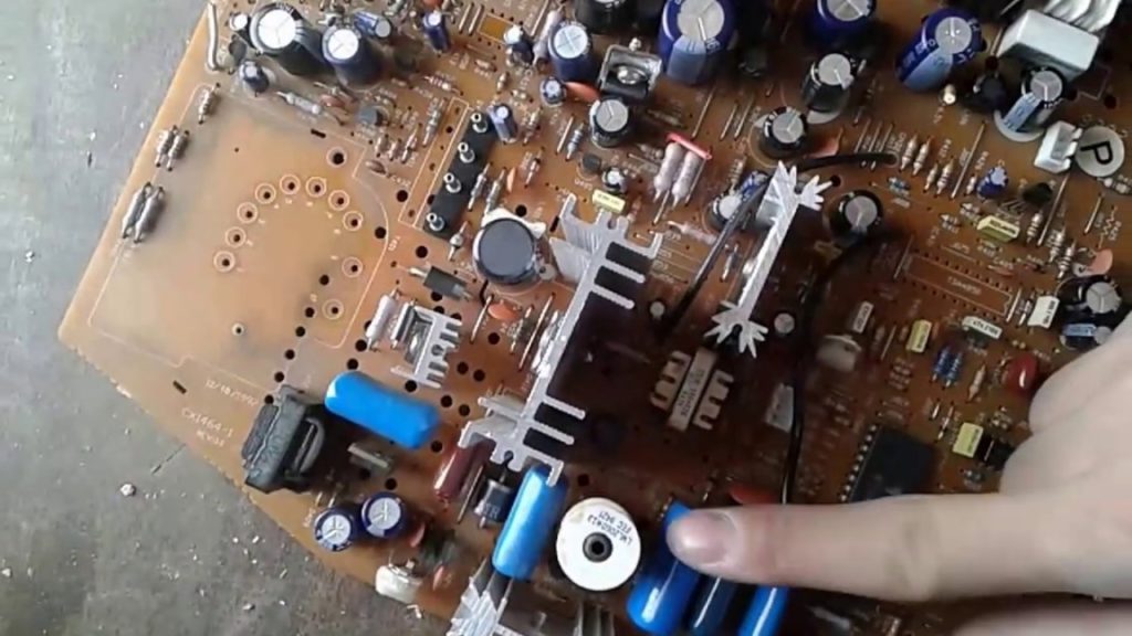
As for those PCB board reverse engineering with high density both in the circuit pattern and hole distribution, through hole become less adaptable to this scenario, since it will waste a lot of space for PCB board layout.
In order to solve this issue in the process of PCB board reverse engineering, the advent of blind and buried vias can not only play the role of through hole connection, but also save a lot of PCB board layout space which can help to make the reverse engineering printed circuit board becomes much easier, more smooth and better. PCB reverse engineering is a long, time consuming and complicate process which will require most of the electronic engineers to understand it thoroughly.
The arrangement of ground line and power supply line can greatly determine the PCB board copying project quality, even if the layout of whole PCB board can be completely perferly, due to the inappropriate layout on the power supply line and ground line can cause interference which deteriorate the product functionality even affect the success rate of electronic product by comprehensive reverse engineering PCB board technology. So electronic engineer should try to keep the noise interference level to the minimum level to ensure the stability of products.Founded in 2004, and 100 percent employee-owned, Circuit Engineering Co.,Ltd. provides a wide range of PCB board Reverse Engineering and manufacturing and support services to original equipment manufacturers across a diverse range of high-tech industries throughout the world wide.
From printed circuit board reverse engineering, manufacture and wire harness production to product assembly, packaging and distribution, Circuit Engineering Co.,Ltd.’s ISO-9001 registered and UL-certified operations supply PCB reverse engineering electronic engineering and manufacturing solutions that are custom crafted for both Fortune-1000 and start-up companies alike.
Circuit Engineering Co.,Ltd.’s Maine-based facilities and workforce of dedicated employee-owners enable an operation that responds and adapts quickly to customer needs for new product introduction, engineering design changes and fulfillment. Circuit Engineering Co.,Ltd. offers transparent, competitive pricing and builds partnerships with customers that contribute to long-term success. The company’s work can be found worldwide in building security systems, solar energy equipment, aircraft instrumentation, industrial laser controls, LED lighting, industrial weather stations, and a host of emerging products from high-tech startups.