"Everything we build starts with design engineering. CECL manufactured boards for one of our products. It went perfectly – a real success.It is really an high quality service they have provided to us!"
By Nile Smith from Sinotech Inc.
“We had several very old device with obsolete boards need to be replaced –through CECL professional service.We got what we needed, and we’ve been using the results of the work without any problem till now.”
By Richard Anderson from TWP system Inc.
"Guys from CECL manufacture PCBs we use in one of our products, a clinometer and we’ve never had a problem with anything. The boards come in, they work. And, their team is very responsive."
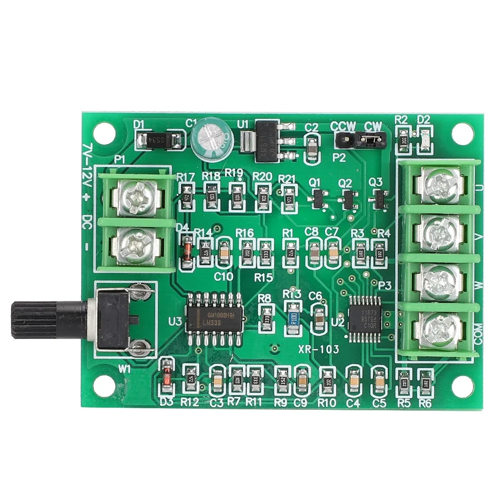
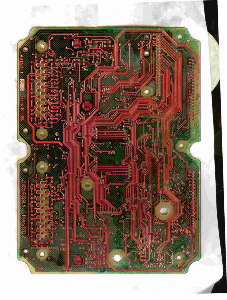
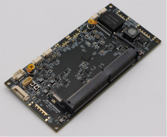
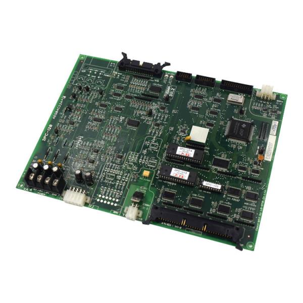
Reverse engineering PCB technology has become an essential capability in modern electronics engineering, especially when dealing with complex systems such as main drive control PCBs. These boards are widely used in industrial automation, motor control, and high-reliability equipment where documentation may be unavailable or outdated. Through advanced reverse engineering processes, engineers can accurately recover critical design data and restore functionality, enabling maintenance, troubleshooting, and long-term lifecycle support. This approach is particularly valuable when original manufacturers no longer provide support or when system upgrades are required.
La rétro-ingénierie des circuits imprimés offre une solution efficace pour prolonger la durée de vie des systèmes électroniques critiques. En exploitant les techniques de rétro-ingénierie, de restauration et de recréation des données de conception essentielles (fichiers Gerber, schémas, plans d’implantation, nomenclatures et netlists), les entreprises peuvent garantir la continuité de leurs opérations et réduire leur dépendance aux fournisseurs d’origine. Qu’il s’agisse de répliquer, de dupliquer ou de repenser entièrement un circuit imprimé de commande de variateur principal, la rétro-ingénierie ne se limite pas à la duplication ; elle s’étend aux processus de remanufacturation, de remise à neuf et de redéveloppement. Pour les circuits imprimés de commande de variateurs principaux, souvent soumis à des charges élevées et à des conditions difficiles, les composants vieillissants et obsolètes peuvent être remplacés par une refonte intelligente. Les ingénieurs peuvent cloner et copier l’architecture d’origine tout en intégrant des composants modernes pour améliorer les performances et la fiabilité.
In the PCB reverse engineering process, layout is the most critical step of circuit board copying, and even there is another saying is all of the work and preparation engineers have done before are all for this purpose. In the whole process of PCB reverse engineering, layout has the high level and most restricted terms, with finest skill and great workload. PCB layout can be separated into single side layout, double side layout and multilayer layout for printed circuit board.
Reverse Engineering von Leiterplatten bietet einen effektiven Weg, die Lebensdauer kritischer elektronischer Systeme zu verlängern. Durch die Nutzung von Reverse-Engineering-Techniken zur Wiederherstellung und Rekonstruktion essenzieller Designdaten – darunter Gerber-Dateien, Schaltpläne, Layoutzeichnungen, Stücklisten und Netzlisten – können Unternehmen die Betriebskontinuität gewährleisten und die Abhängigkeit von den ursprünglichen Zulieferern reduzieren. Ob es um die Replikation, Duplikation oder vollständige Neuentwicklung einer Hauptantriebs-Leiterplatte geht: Reverse Engineering beschränkt sich nicht auf die Duplikation, sondern umfasst auch Wiederaufbereitung, Überholung und Weiterentwicklung. Bei Hauptantriebs-Leiterplatten, die häufig unter hoher Last und rauen Bedingungen arbeiten, können veraltete Komponenten und überholte Teile durch intelligentes Redesign ersetzt werden. Ingenieure können die ursprüngliche Architektur klonen und kopieren und gleichzeitig moderne Komponenten integrieren, um Leistung und Zuverlässigkeit zu verbessern.
Once the physical structure is captured, the next step focuses on logical reconstruction. Engineers analyze signal paths and component functions to develop a complete schematic diagram, effectively translating the physical PCB into an electrical blueprint. Alongside this, a comprehensive BOM list (Bill of Materials) is compiled, identifying all components, specifications, and possible substitutions. These outputs allow engineers to reproduce and duplicate the PCB design, ensuring compatibility with the original system. In many cases, this process also enables improvements, such as component upgrades or design optimization, without compromising system integrity.
La tecnologia di reverse engineering dei PCB offre un potente strumento per estendere il ciclo di vita dei sistemi elettronici critici. Sfruttando tecniche di reverse engineering per ripristinare e ricreare i dati di progettazione essenziali, inclusi file Gerber, schemi elettrici, disegni di layout, distinte base (BOM) e netlist, le aziende possono mantenere la continuità operativa e ridurre la dipendenza dai fornitori originali. Che l’obiettivo sia replicare, duplicare o riprogettare completamente un PCB di controllo principale di un azionamento, il reverse engineering non si limita alla duplicazione, ma si estende ai processi di rigenerazione, ricondizionamento e riprogettazione. Per i PCB di controllo principale degli azionamenti, che spesso operano sotto carichi elevati e in condizioni difficili, i componenti usurati e obsoleti possono essere sostituiti attraverso una riprogettazione intelligente. Gli ingegneri possono clonare e copiare l’architettura originale integrando componenti moderni per migliorare le prestazioni e l’affidabilità.
La ingeniería inversa de la tecnología PCB ofrece una vía eficaz para extender el ciclo de vida de los sistemas electrónicos críticos. Mediante técnicas de ingeniería inversa, restauración y recreación de datos de diseño esenciales (incluidos archivos Gerber, diagramas esquemáticos, planos de diseño, listas de materiales y listas de conexiones), las organizaciones pueden mantener la continuidad operativa y reducir la dependencia de los proveedores originales. Ya sea que el objetivo sea replicar, duplicar o rediseñar por completo una PCB de control de accionamiento principal, la ingeniería inversa no se limita a la duplicación, sino que se extiende a los procesos de remanufactura, reacondicionamiento y rediseño. Para las PCB de control de accionamiento principal, que a menudo operan bajo cargas elevadas y condiciones adversas, los componentes envejecidos y las piezas obsoletas pueden reemplazarse mediante un rediseño inteligente. Los ingenieros pueden clonar y copiar la arquitectura original, integrando al mismo tiempo componentes modernos para mejorar el rendimiento y la fiabilidad.
And there are two ways of PCB design layout: automatically layout and cross layout. Before engineer use automatically layout, they can use cross layout in advance in those circuit parts which has higher requirement. The circuit conductors on the input and output terminate should avoid the parallel layout which can help to decrease the reflection interference. Add ground line to isolate them when necessary and the layout in adjacent layers should be vertical, since parallel could possibly has the decoupling issue.
The first yield rate of automatically layou is firmly depends on the high quality of PCB board circuit pattern arrangement, the layout rules can be set in advance, which include the bend quantity, number of through hole, stepper quantity, etc. generally speaking, exploring stepper should be instrumented first, and then follow the short circuit connection swiftly, finally comes the labyrith layout, so optimize the layout profile is critical.
Tersine mühendislik PCB teknolojisi, kritik elektronik sistemlerin ömrünü uzatmak için güçlü bir yol sunar. Gerber dosyaları, şematik diyagramlar, yerleşim çizimleri, malzeme listeleri ve ağ listeleri de dahil olmak üzere temel tasarım verilerini tersine mühendislik, geri yükleme ve yeniden oluşturma tekniklerinden yararlanarak, kuruluşlar operasyonel sürekliliği sağlayabilir ve orijinal tedarikçilere olan bağımlılığı azaltabilir. Amaç ister ana sürücü kontrol PCB’sini kopyalamak, çoğaltmak veya tamamen yeniden tasarlamak olsun, tersine mühendislik yalnızca çoğaltma ile sınırlı değildir, aynı zamanda yeniden üretim, yenileme ve yeniden geliştirme süreçlerini de kapsar. Genellikle yüksek yük ve zorlu koşullar altında çalışan ana sürücü kontrol PCB’leri için, eskiyen bileşenler ve kullanım dışı parçalar akıllı yeniden tasarım yoluyla değiştirilebilir. Mühendisler, performansı ve güvenilirliği artırmak için modern bileşenleri entegre ederken orijinal mimariyi kopyalayabilir ve çoğaltabilir.
Ultimately, reverse engineering PCB technology provides a powerful pathway to extend the lifecycle of critical electronic systems. By leveraging techniques to reverse engineering, restore, and recreate essential design data—including Gerber files, schematic diagrams, layout drawings, BOM lists, and netlists—organizations can maintain operational continuity and reduce dependency on original suppliers. Whether the goal is to replicate, duplicate, or fully redesign a main drive control PCB, this technology offers a strategic advantage in today’s rapidly evolving electronics landscape.