

Ground Isolation Techniques
While the use of ground planes from Printed Circuit Board Gerber Regeneration does lower impedance and helps greatly in lowering ground noise, there may still be situations where a prohibitive level of noise exists. In such cases, the use of ground error minimization and isolation techniques can be helpful.
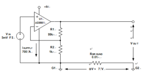
Another illustration of a common-ground impedance coupling problem is shown in below Figure. In this circuit a precision gain-of-100 preamp amplifies a low level signal VIN, using an AD8551 chopper-stabilized amplifier for best dc accuracy. At the load end, the signal VOUT is measured with respect to G2, the local ground. Because of the small 700A ISUPPLY of the AD8551 flowing between G1 and G2, there is a 7V ground error—about 7 times the typical input offset expected from the op amp.
Unless Care Is Taken, Even Small Common Ground Currents Can
This error can be avoided simply by routing the negative supply pin current of the op amp back to star ground G2 as opposed to ground G1, by using a separate trace on the file acquired from Printed Circuit Board Gerber Regeneration process. This step eliminates the G1-G2 path power supply current, and so minimizes the ground leg voltage error. Note that there will be little error developed in the “hot” VOUT lead, so long as the current drain at the load end is small.
In some cases, there may be simply unavoidable ground voltage differences between a source signal and the load point where it is to be measured. Within the context of this “same-board” discussion, this might require rejecting ground error voltages of several tens-of-mV. Or, should the source signal originate from an “off-board” source, then the magnitude of the common-mode voltages to be rejected can easily rise into a several volt range (or even tens-of-volts) after PCB Reverse Engineering.