

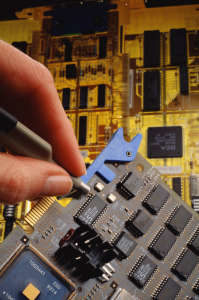
Elements of PCB Board Reverse Engineering
Elements from PCB Board Reverse Engineering represent the components on a board. Elements are loaded from ASCII coded files in a similar manner to the layout file itself, or from the library selector window. An element is composed of lines and arcs on the silk-screen layer (used to define the package outline), pins (or pads for SMD) and three labels that define the description from design rule checking of PCB circuit board reverse engineering, the element’s layout-name (which also appears on the silk-screen layer) and its value.
You can choose which of the names are displayed on the screen with the Screen menu; however, the silk screen in the printout will always show the layout-name. Element pins are contained on the first logical level and so reside on all layers, but the pads of surface-mount elements reside on only the component or solder layers after test structure of PCB Board Reverse Engineering. An element can have a mixture of pins, pads (on one or both sides), and mounting holes.
A mark is used to position the element with respect to the cross hair during pasting. The mark will lie on a grid point when the element is positioned. The mark is drawn as a small diamond shape, but is only visible when both the silk and pins/pads layers from Printed circuit Board Reverse Engineering test coupon guilines are visible. All parts of an element are treated as one unit, except for the name. It is not possible to delete a single pin or move only part of an element on the layout. You can resize separate pieces of an element, but doing so is usually a bad idea. You can move/rotate the element name independently of the element it belongs to. When you move an element name, a line is draw from the cursor to the element mark so it is easy to tell which element the name.
Each pin and pad has two string identifiers, one is the “name” which is a functional description of the pin (e.g. “clock in”) and the other is the “number” of the pin which is used to identify it in a netlist. The “number” is usually an integer, but it can be any string. You can edit the “name” of each pin of an element, but the “number” is embedded in the element definition after PCB Reverse Engineering and is determined when the new element is first created. Pads are similar to lines on a layer but they must be oriented either vertically or horizontally. Pads can have either rounded or square ends. Pins can be round, square, or octagonal.
Tags: pcb board reverse engineering,pcb card reverse engineering,pcb circuit board reverse engineering,pcb reverse engineering,pcba reverse engineering,Printed Circuit Board Reverse Engineering,printed wiring board reverse engineering,pwb reverse engineering,pwba reverse engineering