reverse engineering pcb circuit diagram
-
Record Keeping when Disassembly a PCB
Disassembly a PCB is an critical process when reverse engineering PCB, in order to have the bare PCB board which can scan the TOP & BOTTOM side of PCB board, all the components assemblied on it must be removed properly and clearly. When disassem...
-
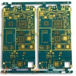
PCB Board Reverse Engineering Component Layout
PCB Board Reverse Engineering Component Layout can be draw which include the footprint, circuitry track pattern, package and location on the whole printed circuit board; PCB Board Reverse Engineering Component Layout can be draw which include the...