

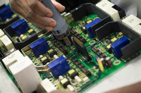
PCB Board Reverse Engineering Component Layout
PCB Board Reverse Engineering Component Layout can be draw which include the footprint, circuitry track pattern, package and location on the whole printed circuit board;
Since most of the Surface mount technology will use the infrared radiation hot wave soldering for the assemble of component, as a result of that, the layout of components will affect the soldering point quality when assembly components over PCB board, and furthermore will affect the finished product success rate.
Electronic magnetic compatibility will require each one of the circuit module to generate as few of the electronic magnetic radiation as possible, and must has a certain kind of the anti-electronic magnetic interference ability.
As a result of that, the layout of electronic components will also directly affect the features of circuit. Consequently, so when reverse engineering the radio frequency PCB card, except the consideration of normal pcb board, how to minimize the mutual interference between each part, how to minimize the interference of Pcb board itself against other circuits also improve its capability to resist the interference.
According to the experience, the effect of radio frequency circuit will not only determined by the feature performance from radio frequency pcb board itself, but most of the interference among the CPU processing PCB. As a result of that, rational layout becomes extremely important in the process of PCB card cloning.
Tags: reverse engineering pcb bom,reverse engineering pcb circuit diagram,reverse engineering pcb data,reverse engineering pcb design,reverse engineering pcb gerber file,reverse engineering pcb layout,reverse engineering pcb part,reverse engineering pcb schematic