

Reverse Engineering Printed Circuit Board Technique
Reverse Engineering Printed Circuit Board Technique
Printed Circuit Board is built as a stack of layer pairs and through the Reverse Engineering Printed Circuit Board Technique we can get the circuitry pattern drawing of each layer, especially for the multi-layers.
Each pair starts as an insulating sheet with copper deposited on one or both sides. The copper sides of the sheet are first etched with different wiring patterns.
Then the sheets are stacked into a sandwich separated by insulating material. Small holes are drilled into the board. Finally, the holes are plated with metal, so that electrical contact is made with each layer that has copper left at hole locations.
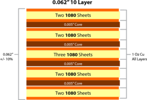
reverse engineering printed circuit board layer pair
Hence, a hole can form a conductive path between two or more layers in the Printed circuit board structure. The standard term used in PCB and chip layout for a hole is via. Parts can be attached to boards in two ways. The classical method is to solder the pins of the components into a via pattern on the board. The other possibility is the utilization of surface mount devices, which are glued to the printed circuit board, surface mount drawing can also be made through Printed circuit board reverse engineering, which is also call the stencil file.
Little connection pads on the devices make contact with their counterparts on the board without penetrating it. Note that the drill holes for vias that are only used to make connections between layers can be much smaller than those holes in which pins must be inserted.
To have a single term we will call the pins and pads of the components terminals. A set of terminals that have to be electrically connected is called a net. chip design it is implicitly understood that the electrical connection has to be realized by a tree (on a routing graph to be described later). This standard definition of a net just specifies the nodes that have to be connected and leaves open how the actual wiring is done. Two different nets (i. e., their physical realization) must be insulated from each other.