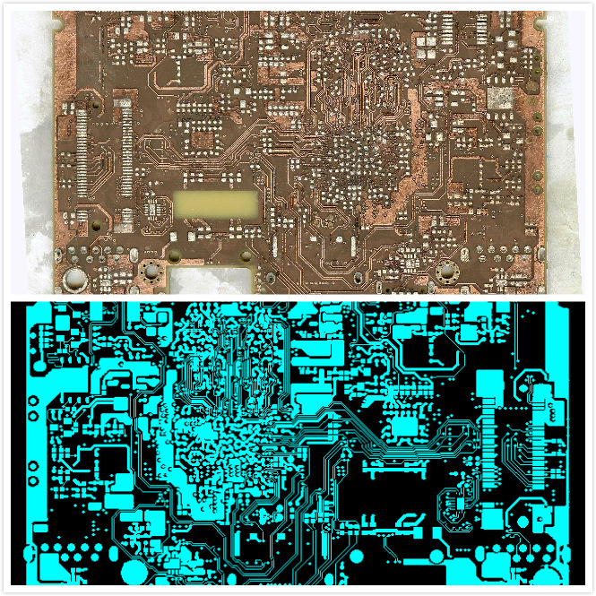
Reverse Engineering Electronic Circuit Board Layout Drawing for Signal Integrity
Reverse Engineering Electronic Circuit Board Layout Drawing for Signal Integrity, and the most frequent signal integrity problems includes mainly include signal reflection, crosstalk, signal delay, and timing errors.
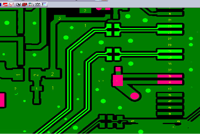
Reflection: When the signal is transmitted on the printed circuit board transmission line, when the characteristic impedance of the transmission line on the high-speed PCB reverse engineering does not match the source impedance or load impedance of the signal, the signal will be reflected, causing overshoot and undershoot in the signal waveform.
Ringing phenomenon. In printed circuit board layout redesign, impedance matching is generally used to prevent reflections. Single-ended 50 ohm.