

Printed Circuit Board Transmission Line
We earlier considered the benefits of outward and return signal paths being close together so that inductance is minimized. When an HF signal flows in a PC track running over a ground plane, the arrangement functions as a microstrip transmission line, and the majority of the return current flows in the ground plane directly underneath the line.
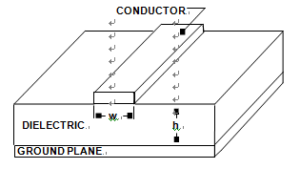
Below Figure shows the general parameters for a microstrip transmission line, given the conductor width, w, dielectric thickness, h, and the dielectric constant, Er. The characteristic impedance of such a microstrip line will depend upon the width of the track and the thickness and dielectric constant of the PCB material. Designs of microstrip lines are covered in more detail later in this chapter.
A PCB Microstrip Transmission Line Is an Example
For most dc and lower frequency applications, the characteristic impedance of PCB traces will be relatively unimportant. Even at frequencies where a track over a ground plane behaves as a transmission line, it is not necessary to worry about its characteristic impedance or proper termination if the free space wavelengths of the frequencies of interest are greater than ten times the length of the line.
However, at VHF and higher frequencies it is possible to use PCB tracks as microstrip lines within properly terminated transmission systems. Typically the microstrip will be designed to match standard coaxial cable impedances, such as 50 Ù, 75 Ù, or 100 Ù, simplifying interfacing.
Note that if losses in such systems are to be minimized, the PCB material must be chosen for low/high frequency losses. This usually means the use of Teflon or some other comparably low-loss PCB material. Often, though, the losses in short lines on cheap glass-fiber board are small enough to be quite acceptable.