

Printed Circuit Board Wiring Diagram Reverse Engineering
The main parasitic elements generated by printed circuit board wiring diagram reverse engineering include: parasitic resistance, parasitic capacitance and parasitic inductance.
For example: the parasitic resistance of the PCB is formed by the traces between the components;
The traces, pads and flat traces on the circuit board will generate parasitic capacitance; the parasitic inductance from circuit board cloning is generated by loop inductance, mutual inductance and vias.
When converting the circuit schematic into an actual PCB, all these parasitic elements may interfere with the effectiveness of the circuit.
This article will quantify the most difficult type of circuit board parasitic components—parasitic capacitance, and provide an example that can clearly see the impact of parasitic capacitance on circuit board performance.
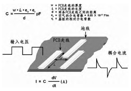
Placing two traces close together on the PCB can easily generate parasitic capacitance. Due to the existence of this parasitic capacitance, a rapid voltage change on one trace will generate a current signal on the other trace.