

Circuit Board Parasitic Inductance Cloning Principle
Circuit Board Parasitic Inductance Cloning Principle is similar to that of parasitic capacitance. It is also to layout two traces when reverse engineering electronic circuit board design. On two different layers, place one trace on top of the other trace; or on the same layer, place one trace next to the other, as shown in below Figure.
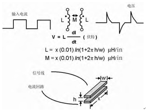
In these two trace configurations, the current on a trace changes with time (dI/dt). Due to the inductance of this trace, voltage will be generated on the same trace; and due to the existence of mutual stray inductance, it will A proportional current is generated on the other trace.
If the voltage change on the first trace is large enough, interference may reduce the voltage tolerance of the high speed digital circuit and cause errors. This phenomenon does not only occur in digital circuits, but this phenomenon is more common in digital circuits because of the large instantaneous switching currents in digital circuits.