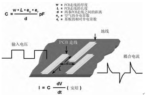
Reverse Engineering Electronic Circuit Board Layout Design
The most commonly used technique of reverse engineering electronic circuit board layout design is to change the size between traces according to the capacitance equation. The most effective size to change is the distance between the two traces.
It should be noted that the variable “D” is in the denominator of the capacitance equation. As “D” increases, the capacitive reactance decreases. Another variable that can be changed is the length of the two traces.
In this case, as the length “L” decreases, the capacitive reactance between the two traces will also decrease. Another technique is to reverse engineering PCB board ground wire layout between these two traces.
The ground wire of fuel ignition controller is low impedance, and adding another trace like this will weaken the interference electric field, as shown in below Figure.