

Printed Circuit Board Reverse Engineering Inspection
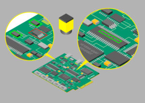
In order to complete the inspection, there is a great variety of inspection facilities has been invented. Automatic optical inspection system can inspect the internal layer before the stack up process; after the pressing process done, X ray system can monitor the preciseness of registration and alignment as well as the minor flaw; scanning laser system provide the inspection method for soldering pad of Printed circuit board Reverse Engineering before reflow process. All of these systems plus the direct visual inspection and integrity inspection of component placement on the printed circuit board reverse engineering line can serve to ensure the final reverse engineering and soldering printed circuit board reliability.
However, even all of these efforts can decrease the rate of flaw to the minimize level, we still need to proceed the final inspection, which could probably the most important thing since it is the final unit of the whole process for evaluation.
Printed Circuit Board Reverse Engineering Inspection
The final inspection can be completed manually or through the automatic system, and most of time it should be done by these two methods simultaneously. Manually operation means visual inspection of pcb plate reverse engineering by operator using optical facility, and make the right judgment about the flaw. Automatically system define the flaw by computer assistant graphic analysis. Some people believe that automatic system include all the inspection methods except manual visual inspection of printed circuit board reverse engineering.
X ray technology is a kind of method provide information about printed circuit board solder tin thickness, dissipation, internal hole and crack, cold soldering of printed circuit board and solder ball existence. Ultrasonic can inspect the voids, crack and other unattached joint on PCB reverse engineering. Automatically inspection can estimate the external cosmetic performance like bridge, tin capacity and shape on the printed circuit board. Laser scanning can provide the external features of three dimension graphics. Red radiation inspection can detect compare the already known well soldered point and then detect if there is any defect on the another soldering point if the heating signal is abnormal.
Tags: pcb assemble reverse engineering,pcb board reverse engineering,pcb card reverse engineering,pcb reverse engineering,pcba reverse engineering,Printed Circuit Board Reverse Engineering,printed wiring board reverse engineering,pwb reverse engineering,pwba reverse engineering