

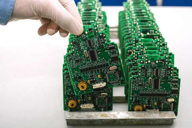
Printed Circuit Board Reverse Engineering Horizontal Standardization
Printed Circuit Board Reverse Engineering Horizontal Standardization will effectively help to improve the accuracy and progress of PCB reverse engineering through which the layout drawing, Gerber file, Bill of material and schematic diagram can be extracted;
The horizontal offset of the CITS500s from PCB reverse engineering and its cable should be standardized to ensure that any CITS500s system will measure the same region of the coupon waveform, and that errors are not introduced due to cables having different physical and electrical lengths.
Select Learn Cable Length from the Utilities menu if printed circuit board reverse engineering Connect the working probe cable, without the probe, to the MAIN SMA front panel connector. Press the Learn Cable Length button. The CITS will determine the length of the cable, and display the time difference from the nominal length after circuit board copying.
If the time difference exceeds ±10 ps press Apply Correction to adjust the system calibration. Use the CITS500s Test File editor to create a test specification for each test trace on the test coupon. “Probe Length” specifies the total electrical length of the microstrip probe and its cable. (Usually a slightly smaller value is used so that poor quality probe-to-test-trace connections can be viewed in the display screen.)
The “Test From” and “Test To” limits define the tested area of the coupon trace (see below). This is usually the flattest part of the waveform and is referred to as the undisturbed interval. Typical sets of parameters are shown on the following pages. These may need to be adjusted depending on the type of cable and probe being used and the length of the coupon trace under test.
The tested area is usually the flattest portion of the coupon waveform and is usually referred to as the undisturbed interval. Ignore test connection aberrations and open circuit termination effects if pcb board copying.
Select the “Test From” and “Test To” limits to test the undisturbed interval.
Tags: pcb assemble reverse engineering,pcb board reverse engineering,pcb card reverse engineering,pcb reverse engineering,pcba reverse engineering,Printed Circuit Board Reverse Engineering,printed wiring board reverse engineering,pwb reverse engineering,pwba reverse engineering