

Inkjet Printer PCB Board Copy
After you get started of your Inkjet Printer PCB Board Copy project with us, all the necessary files include layout drawing, gerber file, bill of material and schematic diagram will be submitted in below format through which your inkjet printer PCB board can be remanufacture and assembly anywhere in the world, we can ensure the accuracy of your data by means of prototype running.
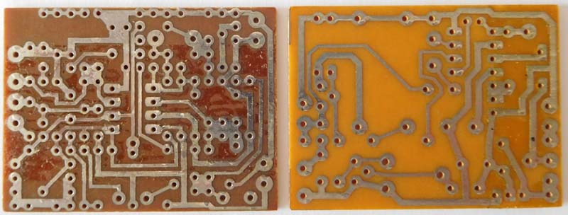
The PCB layout is a digital representation of the physical board, showing the placement of components, traces, and connections. To copy an inkjet printer PCB:
- Scan the PCB: Use high-resolution imaging to capture the board’s layers.
- Trace Mapping: Reverse-engineer the copper traces and component placements.
- Software Tools: Use Altium Designer, KiCad, or Eagle to recreate the layout.
A well-documented PCB layout ensures accurate replication and helps in troubleshooting printer malfunctions.
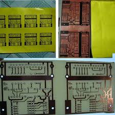
Gerber files are industry-standard formats used for PCB manufacturing. They include:
- Copper layers (top/bottom traces)
- Silkscreen (component labels)
- Solder mask (insulating layer)
- Drill files (hole placements)
The BOM list details all components on the inkjet printer PCB, including:
- Resistors, capacitors, diodes
- ICs (Integrated Circuits)
- Connectors & transistors
- Other passive/active components
A complete BOM helps in sourcing replacement parts and ensures the new PCB functions identically to the original.
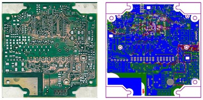
The schematic diagram is a circuit blueprint showing electrical connections between components. Steps to extract it:
- Analyze PCB traces to map connections.
- Identify components and their relationships.
- Use CAD tools (like OrCAD or Proteus) to draw the schematic.
A correct schematic ensures the copied PCB operates with the same logic as the original inkjet printer board.
Copying an inkjet printer PCB requires expertise in reverse engineering to generate accurate layout drawings, Gerber files, BOM lists, and schematic diagrams. These files are essential for repair, mass production, or upgrading printer circuit boards. With the right tools and methodology, PCB board copying can save costs and extend the lifespan of printing devices.
Here is sample of files and drawings after copy 4 layers Inkjet Printer PCB board by PCB reverse engineering technique you will receive, based on a typical 4 layer Inkjet PCB Board copy with components mounted on two sides:
1st Grounding layer of Gerber Files from Inkjet Printer PCB board:

2nd Grounding layer of Gerber Files from Inkjet Printer PCB board:

BOTTOM layer of Gerber Files from Inkjet Printer PCB board:

TOP layer of Gerber Files from Inkjet Printer PCB board:

Schematic Diagram from Inkjet Printer PCB board:

Circuit Engineering Company Limited provide a complete PCB Reverse Engineering, PCB Clone and PCB Replicate service, Rapid Prototyping and functional test services using the latest technologies combined with traditional skills for a wide range of industries. By integrating our traditional skills with the latest technologies, we can offer clients a comprehensive portfolio of product development services all under one roof. For more details please contact our customer service team.
Tags: обратно инженерство pcb layout