

Power Supplies PCB Board Schematic Cloning
The Power Supplies PCB Board Schematic is an important part of an electronic product, and Power Supplies PCB Board Schematic Cloning is directly related to the performance of the product.
The Power Supplies Printed Circuit Board gerber file and schematic diagram of our electronic products mainly include linear power supplies and high-frequency switching power supplies.
Theoretically speaking, the linear power supply is how much current the user needs, and how much current the input terminal must provide; The switching power supply is how much power the user needs, and how much power is provided at the input end.
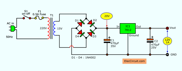
Linear power supply power devices work in a linear state, such as our commonly used voltage regulator chips LM7805, LM317, SPX1117, etc. The following figure 1 is the schematic diagram of the LM7805 regulated power supply circuit:
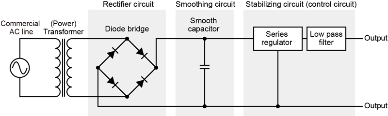
It can be seen from the above figure that the linear power supply is composed of functional components such as rectification, filtering, voltage stabilization, and energy storage. At the same time, the general linear power supply is a series regulated power supply ups circuit board clone, and the output current is equal to the input current. I1=I2 I3, I3 is the reference terminal , the current is very small, so I1≈I3.
Why we talk about current is because the width of each line is not set randomly during power supply PCB design reverse engineering, but is determined according to the current size between component nodes in the schematic diagram (please check “power supply PCB Design reverse engineering Copper Platinum Thickness, Line Width and Current Relationship Table”). The size of the current and the direction of the current flow must be clarified to make the pc board just right;