

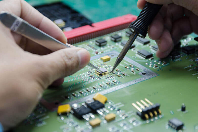
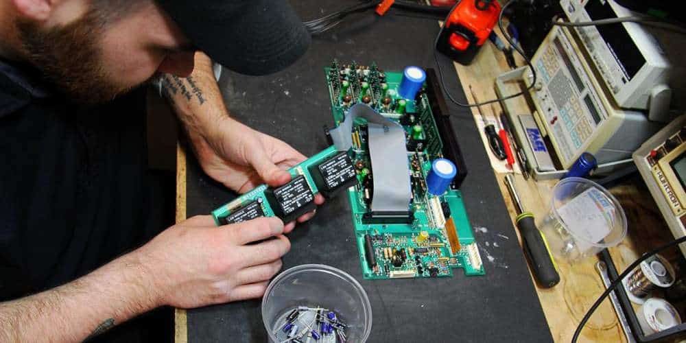
PCB Card Reverse Engineering Solution

When the process of PCB Card reverse engineering has been done, it has been approved that even if the schematic is correct, the electronic device reliability will be doubted is not well. For example, if the two parallel lines very close to each other, will cause the delay of signal wave transmission, and generate the reflect noise at the end of transmitting line;
Interference caused by inappropriate consideration of power supply, grounding will degrade the performance of product. As a result of that, when reverse engineering PCB card, proper PCB reverse engineering measure must be taken to ensure all the switch power supply can have four current reflow:
1> Power supply switch alternative reflow;
2> Output rectification reflow;
3> Input signal source current reflow;
4> Output overload current reflow;
Input reflow charge the capacitor on the PCB card through direct current resemble when reverse engineering PCB card, wave filtering capacitor play the role of wide band energy storage functions. Similarly, output wave filtering capacitor can be used to store the high frequency energy comes from the rectifier, and eliminate the DC energy of output overload reflow.
Consequently, output and input wave filtering capacitor wire connection point is critical, if the output/input current reflow and power supply switch fail to connect with connecting point of capacitor, alternative energy can radiate to environment through output or input wave filtering capacitor.
Tags: pcb assemble reverse engineering,pcb board reverse engineering,pcb card reverse engineering,pcb reverse engineering,pcba reverse engineering,Printed Circuit Board Reverse Engineering,printed wiring board reverse engineering,pwb reverse engineering,pwba reverse engineering