

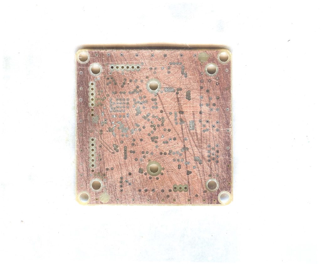
PCB Card Reverse Engineering Data File
PCB Card Reverse Engineering Data File includes all data files for the circuits that are used by the demo layout. The elements in the LED example are not found in the library, but you can lift them from the example itself if you want. If you have problems with the color of the cross hair, change the resource cross hairColor setting to a different one.
Now load a second circuit, the MC68882 FPU for example. Create the circuit as explained above. You now have two different unnamed elements when pcb board reverse engineering. Unnamed means that the layout-name of the element hasn’t been set yet. Selecting description from the Display menu displays the description string of the two circuits which are CPU and FPU.
The values of the circuits are set to MC68030 and MC68882 from pcb card reverse engineering. Each of the names of an element may be changed by <Key>n at the elements location and editing the old name in the bottom input line. Naming pins and vias is similar to elements. You can hide the element name so that it won’t appear on the board silkscreen by pressing <key>h with the cursor over the element. Doing so again un-hides the element name.
Entering :le and selecting an element data file is the second way to load circuits. The third way to create a new element is to copy an existing one PCB board. The fourth way of pcb cloning to create a new element is to convert a buffer’s contents into an element.
Here’s how it’s done: Select the Via-tool from the Tool pallet. Set the grid spacing to something appropriate for the element pin spacing. Now create a series of vias where the pins go. Create them in pin number order. It is often handy to place a reference point (!Ctrl<Key>m ) in the center of the first pin in order to measure the location of the other pins.
Next make a solder-side layer the active layer from the active-layer popup menu. Now draw the outline of the element using lines and arcs. When you’re done, select everything that makes up the element with a box selection (<Btn3Down> drag, <Btn3Up>). Now select “cut selection to buffer” from the Buffer menu.
Tags: replicate pcb card artwork,replicate pcb card bom,replicate pcb card component list,replicate pcb card design,replicate pcb card gerber file,replicate pcb card layout,replicate pcb card part list,replicate pcb card schematic diagram