

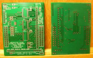
PCB Board Reverse Engineering Inspection
PCB Board Reverse Engineering Inspection includes the inspection against track on top and bottom layer and tracks on the power supply and signal transmission, as well as the soldering pad and socket/terminals/marks:
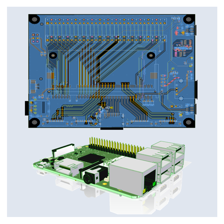
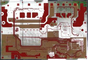
1. the important tracks of top and bottom side pcb board connection need to use not only the insert component but also the through vias;
inspecionar o resultado do desenho de layout da placa PCB, arquivo gerber, diagrama esquemático e documentos da lista BOM por tecnologia de engenharia reversa
2. power supply and signal tracks arrangement in the socket must ensure the signal integrity and anti-interference;
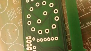
3. take care of the solder pad and solder hole aspect ratio;
проверить результат чертежа печатной платы, файла Gerber, принципиальной схемы и документов списка спецификаций с помощью технологии обратного проектирования
4. ensure all the sockets and terminal are all designed and reverse engineering on the edge of pcb board;
5. check if all the marking on the components are compatible with physical ones, all the components should be reverse engineering towards the same direction and keep in order;
6. increase the width of power supply and grounding tracks as much as possible but within the regulation;
7. generally, upside layer reverse engineering vertical tracks, and downside layer reverse engineering horizontal tracks and ensure the chamfer not less than 90 degree;
با استفاده از فناوری مهندسی معکوس، نتیجه طراحی صفحه برد PCB، فایل ژربر، نمودار شماتیک و اسناد لیست BOM را بررسی کنید.
8. if the quantity and dissipation of tooling holes are proper to decrease the pcb board bend force;
Circuit Engineering Co.,Ltd. is a leading provider of electronic PCB Board Reverse Engineering and manufacturing services incorporating design, PCB assembly, box build, global supply chain management and integrated technologies.
With specialist knowledge of integrated design and manufacturing solutions for high technology, high mix and complex products, we offer a complete service from PCB board reverse engineering, design (electronic, mechanical and software), prototype, new product introduction (NPI), global procurement, in house tooling and moulding, PCB assembly, box build and test, packaging and global logistics.
Our design and engineering expertise – from product design based on customer concept through to re-engineering of existing assemblies – provides comprehensive design support throughout your product life cycle.
With a choice of manufacturing location to suit your volume and technology requirements, we provide global procurement and cost effective sourcing through wholly owned facilities in the Asia.
As a strategic design and manufacturing partner, we provide a complete end-to-end managed solution delivering your product on time and on budget.