

PCB Board Component Placement Location
PCB Board Component Placement Location should first be considered from the PCB Board circuitry schematic diagram to cater to the direction of the circuit board design.
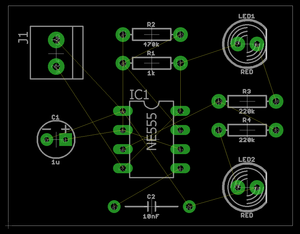
Whether the placement is reasonable or not will directly affect the performance of the printed circuit board, especially for high-frequency analog circuits. Obviously, the location and placement requirements of the device are more stringent.
Therefore, when engineers start to redesign the layout of the printed circuit board and determine the overall layout, they should perform a detailed analysis of the circuit principle, first determine the location of special components (such as large-scale ICs, high-power tubes, signal sources, etc.), and then arrange other components and try to avoid factors that may cause interference.
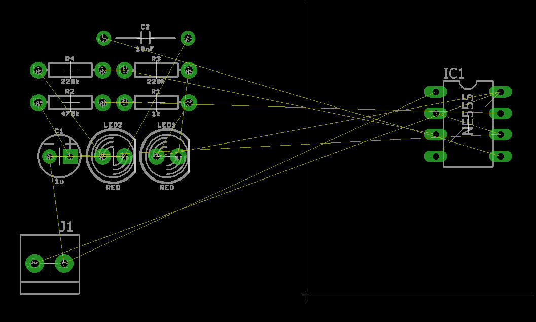
On the other hand, it should be considered from the overall structure of the printed board to avoid uneven and disordered arrangement of components. This not only affects the beauty of the printed board, but also brings a lot of inconvenience to assembly and maintenance work.